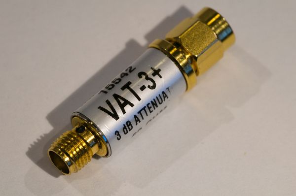
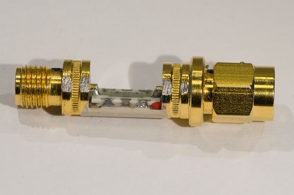
I came across a broken 3 dB attenuator and since I was curious of its internal design, I decided to do an autopsy, just like I did with the broken termination a few months ago. The attenuator is made by Mini-Circuits and it is a low-cost type useful up to 6 GHz. The manufacturer part number is VAT-3+. The data sheet says it costs $13.95.
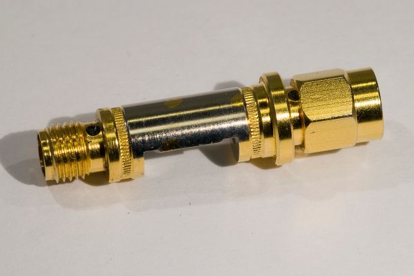
The symptoms were that the female connector was an open circuit (bad) while the male connector had a resistance of 150 ohms to ground (which is what it should be for a 3 dB attenuator). This indicated an open circuit between the female connector and the internal resistive network.
It is perhaps not obvious how to take the attenuator apart, but I decided to start filing on the central tube (which seemed to be made out of brass) in the hope that I would then be able to pry it apart to reveal the interior.
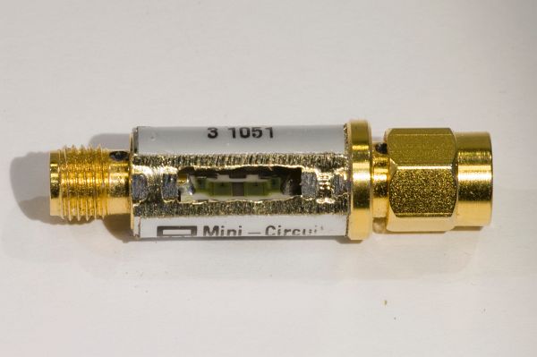
This turned out to be successful and I could soon remove the tube. An alternative (maybe easier?) method might have been to remove the label and then drill out the four punch marks around the rims of the tube.
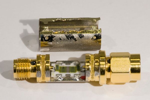
Inside the attenuator, there is a small substrate with four laser trimmed thick film resistors forming the pi-topology attenuator. See my article about pi and T attenuators for more information about attenuator design.
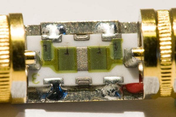
At first glance it was not obvious what was broken inside the device, but there had to be a crack or something between the left connector terminal and the substrate in the photo above. If one looks carefully, it is possible to see that there is indeed a crack around the solder joint. The photo below shows a zoomed in version where the microscopic crack is quite visible.
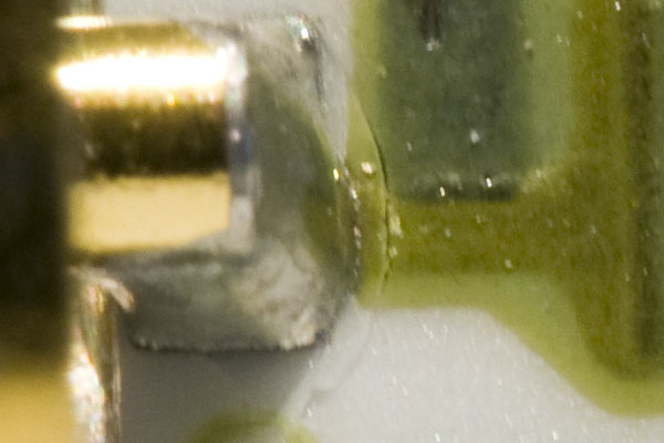
A possible cause for the crack is if an SMA connector with a misaligned center pin was forced into the connector of the attenuator, causing the terminal to be pushed harder towards the substrate than what it could handle.
So, this is what Mini-Circuits’ low-cost 1 W attenuators look like inside. A custom machined brass body onto which a substrate with laser trimmed resistors are mounted.