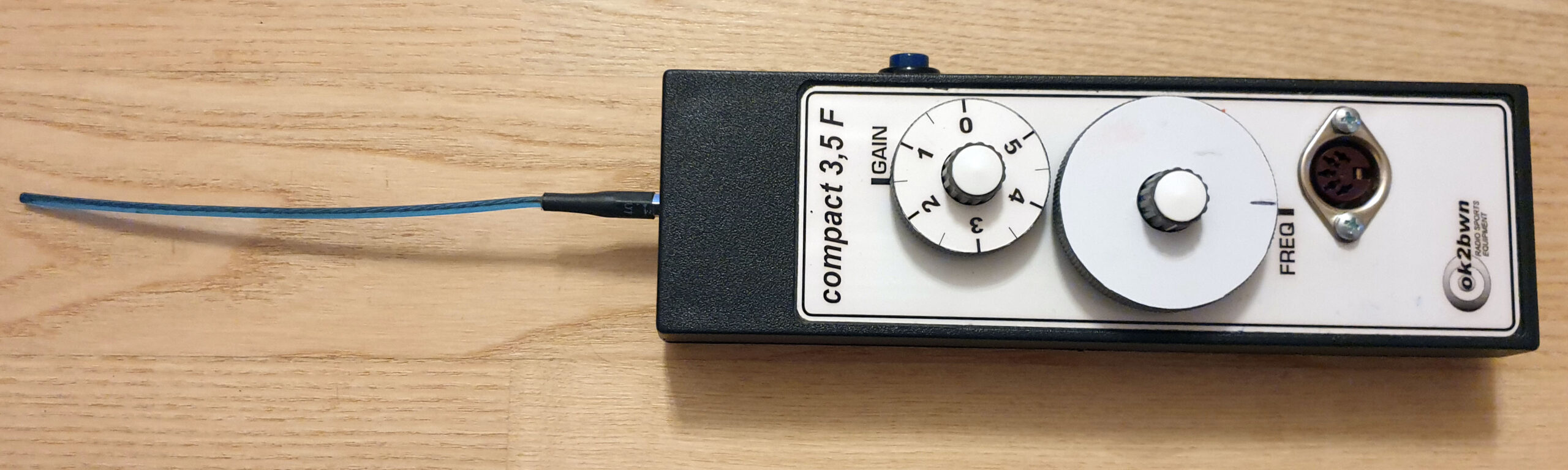
I maintain a set of simple ARDF (amateur radio direction finding, or “fox hunting”) receivers of the type Compact 3,5F from OK2BWN for use by beginners. A problem with some of the receivers is that the gain cannot be set low enough, which means that the audio becomes unbearably loud close to a transmitter. I could not find any schematics online, so I decided to reverse-engineer the receiver so that I could figure out what to change to allow lower gain.
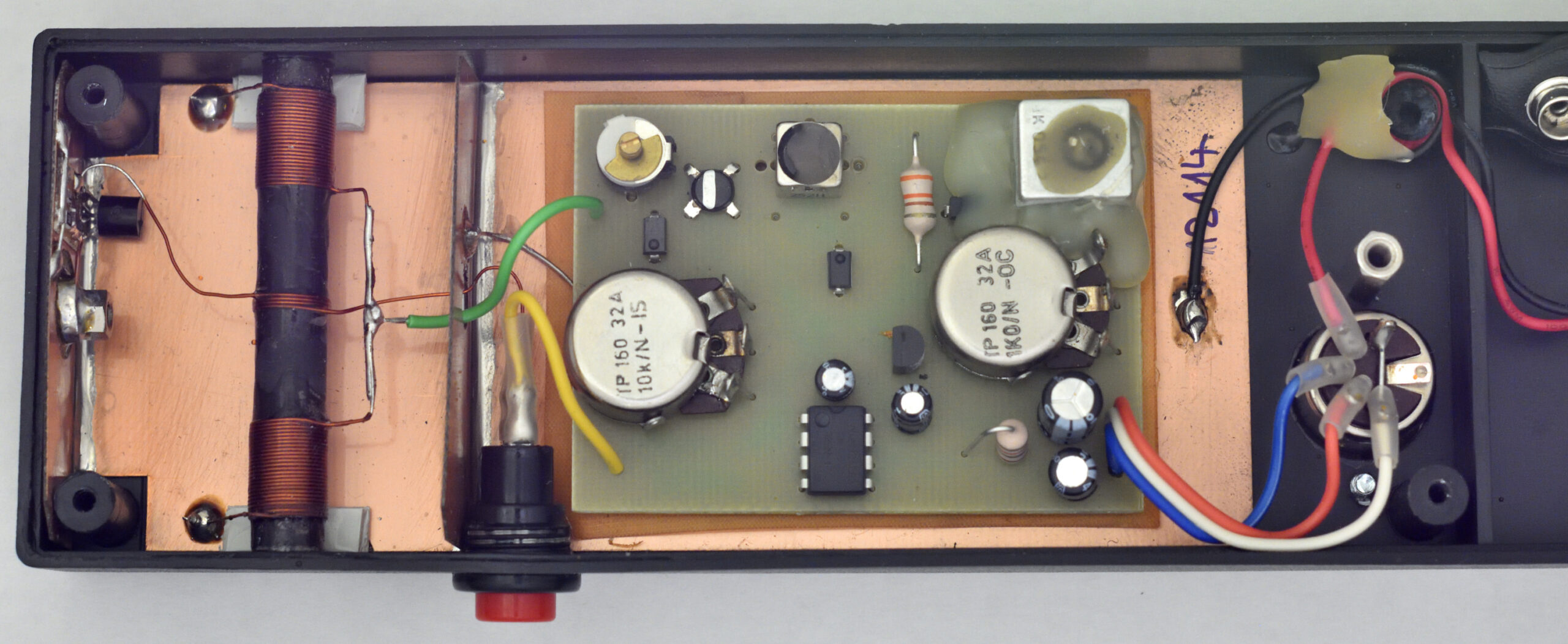
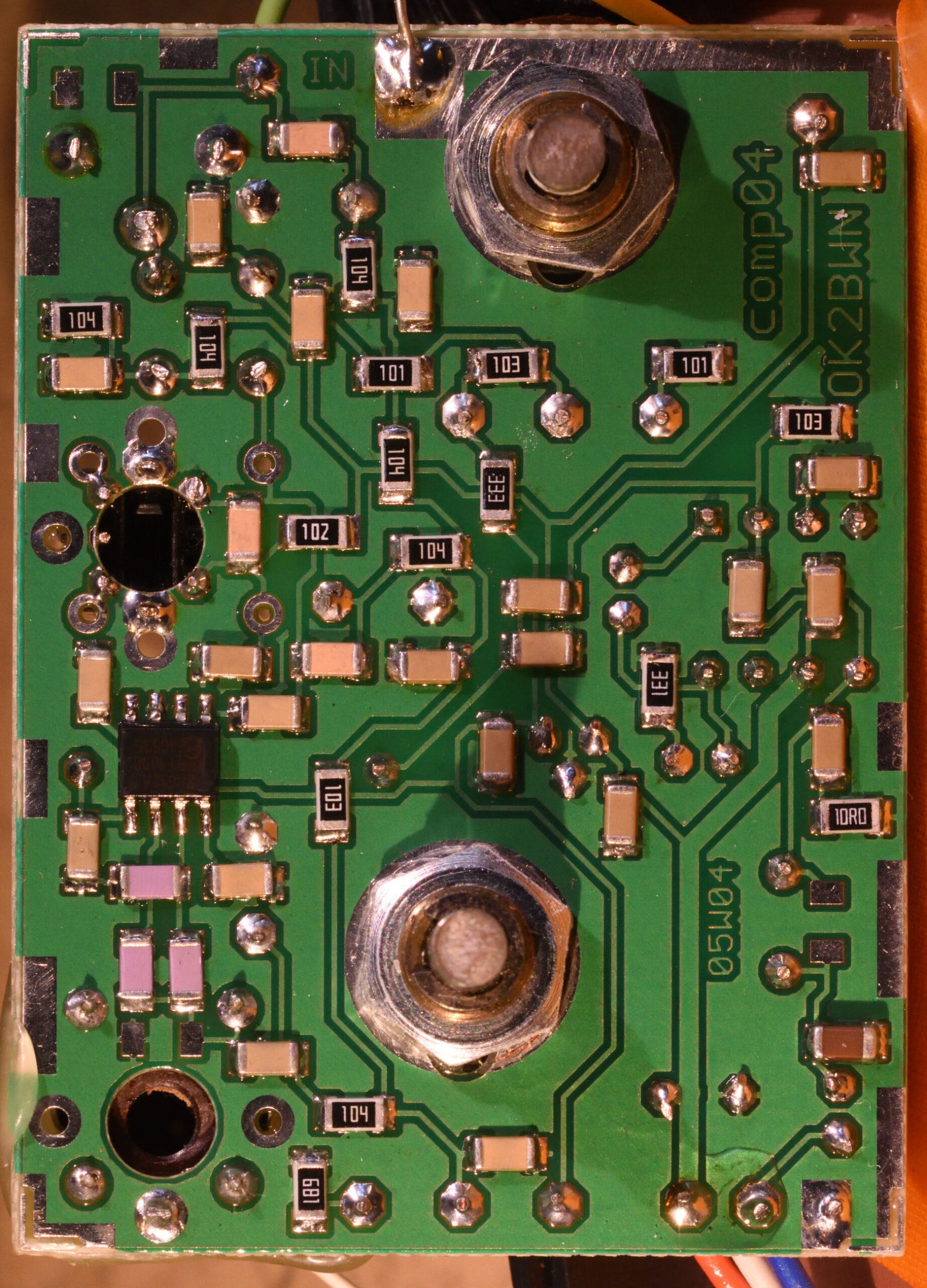
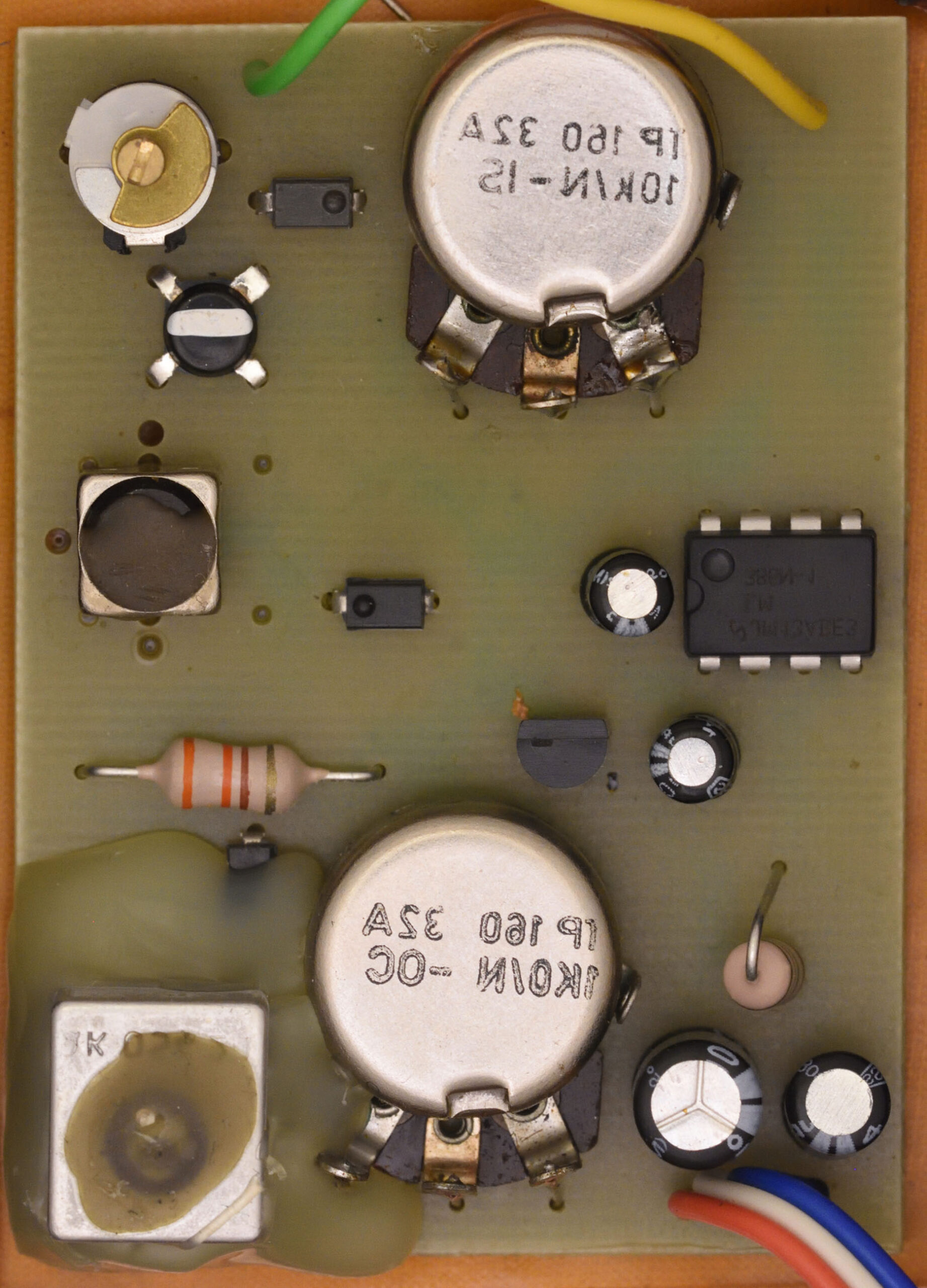
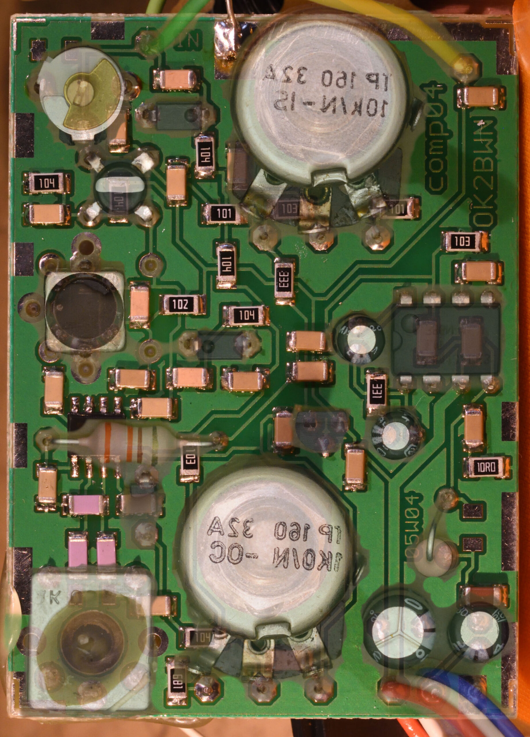
The receiver is built on a single-layer board using some through-hole components on the top side and surface mount components on the bottom. The discrete SMD components are large (1206 size), so the resistors have their values printed on them. This all makes the tracing of the circuitry relatively simple. I photographed both sides, flipped the photo of the top side and overlayed them. Then it was “just” a matter of sketching out the circuitry, a process that involved a couple of false starts before it all converged to something that looks like a direct conversion receiver.
Even before starting, I had a good idea of the general architecture as the receiver contained a single SA612 mixer with an analog VCO and an LM386 audio amplifier, but no crystal or ceramic IF filters (so it was not a superheterodyne). Since there was only one mixer it also could not be an image reject receiver, hence receiving both the desired and undesired sideband, which is also evident when tuning the receiver as a CW signal appears for two different tuning settings close to each other. Another thing that was obvious from using the receiver and looking at the parts inside, was that the signal from the E-field antenna was combined with the signal from the H-field antenna by a few turns on the ferrite core when the “antenna selector” switch was pushed to power the E-field amplifier located on a separate board.
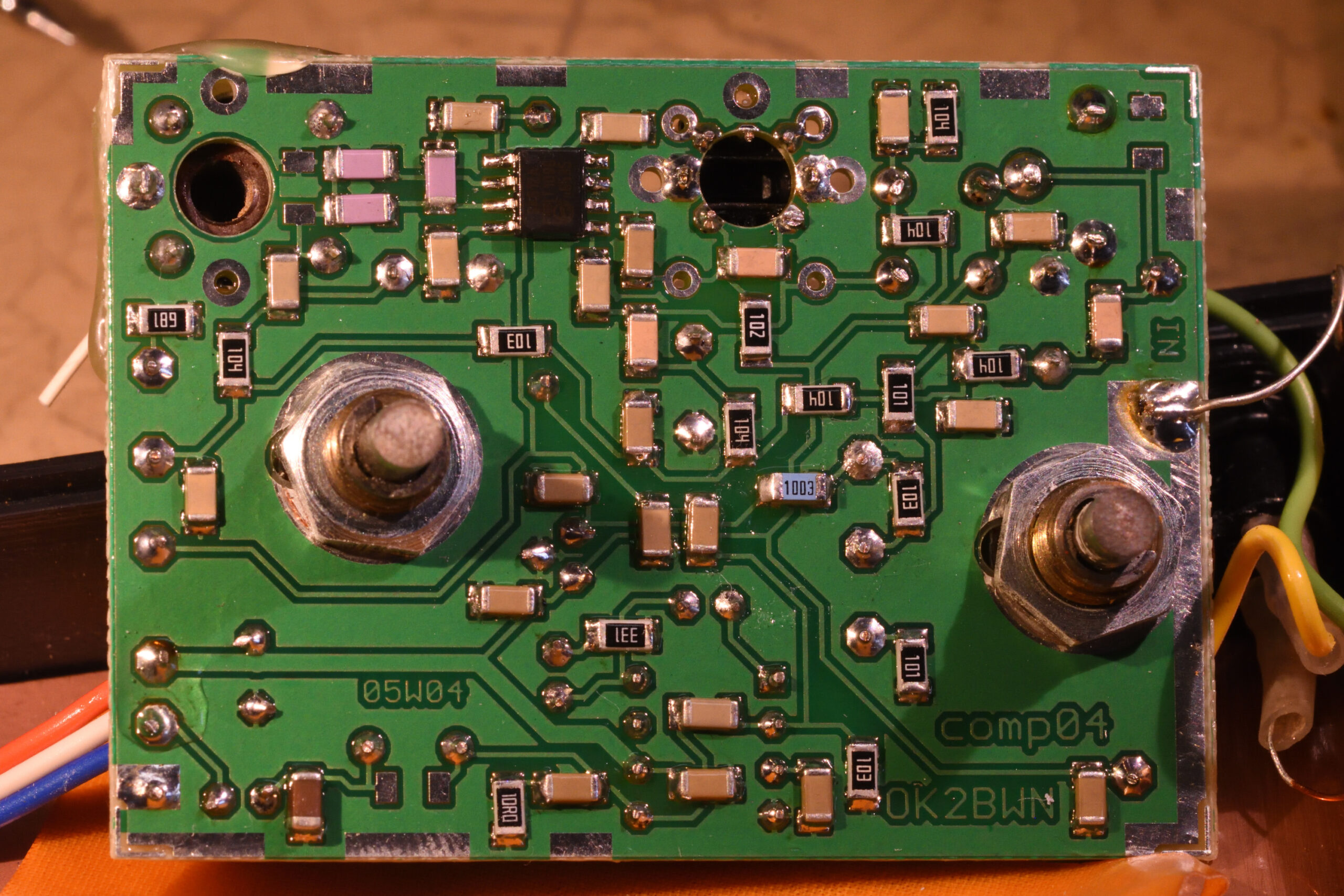
Below are the photos of the top and the bottom of the board, as well as a combined photo where the flipped top side components are shown somewhat transparently over the bottom side photo.
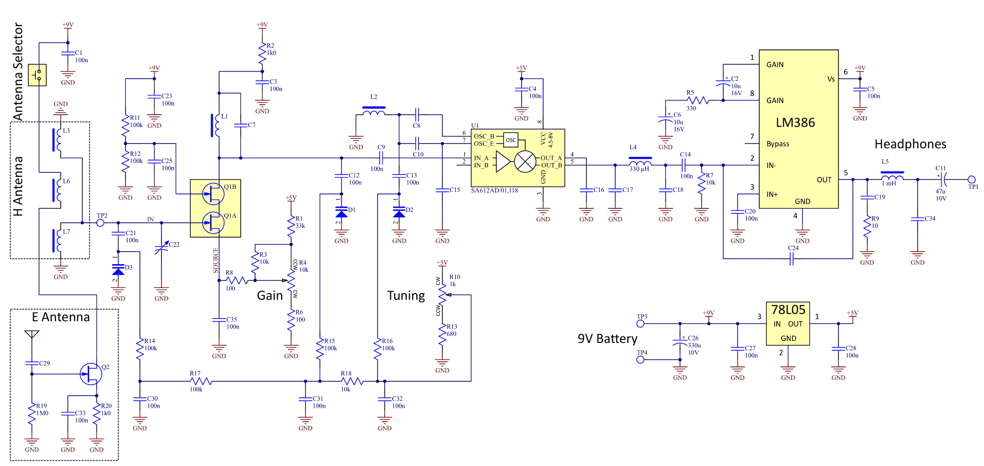
Below is the schematics I came up with. As far as I know, it is correct, but I give no guarantees.
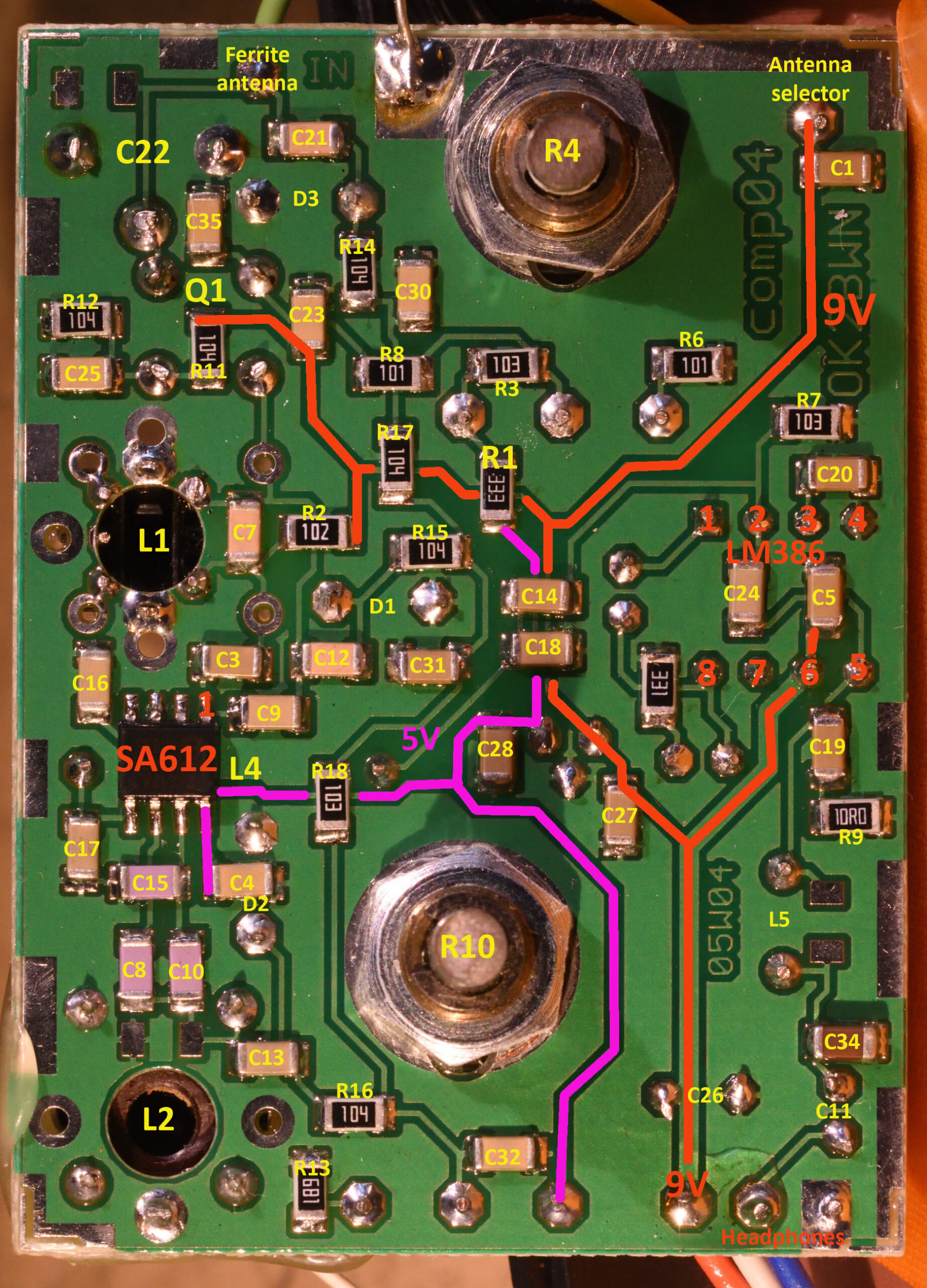
An annotated photo of the bottom of the board is shown below.
I have not bothered to desolder and measure unmarked components like capacitors, so apart from the electrolytics, I do not know their values. I wrote 100 nF on capacitors I think only serve the function of DC-blocks, supply decoupling or low-pass filtering of the varactor bias, but this is just a guess. They could have some other value, although that is unlikely to be critical. The capacitors in series with the varactors might theoretically have some low value to adjust/reduce the tuning range, so there the 100 nF guess could be more wrong.
There are a few mystery components in the circuit. The four-pin through-hole part (Q1A, Q1B in the schematic) near the antenna is unmarked, except for a white stripe. Based on its place in the circuit and the components around it, I have guessed it is a double JFET in cascode configuration. While there are indeed dual JFETs available today, I could not find one with this package. My guess is that it is an obsolete part. Also, the varactors are unmarked, but the conclusion they are varactors is more solid than the guess regarding the dual JFET.
A JFET cascode amplifier is a good choice as a low-noise-amplifier for a ferrite antenna as it has high input impedance and low noise. Here it has a tuned drain circuit which increases the gain at the cost of some added complexity (and risk of oscillation?). The Q is limited by the 1.5 kohm input impedance of the SA612.
I suppose having a tuned RF amplifier was necessary to get enough gain for weak signals. The other gain elements are the mixer (nominally 14 dB) and the LM386. The RF amplifier is the only adjustable gain element in the receiver, which is perhaps an unusual choice. The input gate is DC-biased to 0 V via the ferrite antenna while the source is connected to a decoupled (C35) resistive network around the gain potentiometer, which allows changing the operating point of the JFET to select a suitably steep part of the ID-VGS curve to get the desired gain.
Adjusting the minimum gain
Now that we have the schematics, what do we need to do to allow more attenuation/less gain? The obvious place to look is near the existing gain control circuit. When potentiometer R4 is at its maximum counter-clockwise (CCW) position, the gate-source of JFET Q1A is maximally back biased to operate at the shallowest ID-VGS point and thus lowest gain. But we need it to be lower still.
VGS(off), i.e. the (negative) voltage from gate to source of a JFET required to turn the transistor fully off is not a well-controlled parameter. It can easily vary by a factor larger than two (sometimes larger than five) between devices with the same part number. As discussed the way gain is adjusted in this receiver is largely by adjusting VGS, so it is no surprise that different receivers will have different minimum gains.
To reduce the minimum gain for a receiver, it is fortunately quite easy to make a modification that results in a more negative VGS when the gain pot is maximally turned CCW. Just reduce R1 that together with the gain pot R4 (and R3 and R6) forms a voltage divider from +5V. A lower R1 value means the source will be biased to a higher voltage when the gain pot is at max CCW, but it will have very little effect when the pot is at the opposite end.
I found that parallelling the 33 kΩ R1 with 100 kΩ to get 24.8 kΩ resulted in a decent minimum gain for most receivers I modified. One receiver that was not quite as bad received 130 kΩ across R1 (26.3 kΩ total).
Below is a photo of a board with a blue 100 kΩ resistor soldered on top of the 33 kΩ R1 that was there originally.
Further comments and observations
The antenna is wound using two parallel and mirrored windings. This is supposed to eliminate any possibility of direction error. A direction-finding ferrite antenna should have a null exactly when the magnetic field-lines enter perpendicular to the core, but if there is a single winding on the core with some distance between the start and end of winding, there will be one effective turn over a part of the broadside ferrite core, leading to a slight offset in the null. How big a problem this is in practice is a bit unclear, but it generally is considered good practice to use two windings in parallel, wound symmetrically in opposite directions to cancel this parasitic broadside turn.
There are three varactor-tuned circuits in the receiver that need to be simultaneously tuned to the same frequency as set by the tuning knob: The antenna, the low-noise amplifier and the local oscillator. Getting all three circuits to agree on the frequency for all settings of the tuning dial might have been a challenge when designing the receiver. There is a trimmer capacitor across the antenna that can be adjusted to ensure the antenna agrees with the LO for at least one frequency and the two inductors are also trimmable to allow alignment on at least one (mid-band) frequency. And maybe it is not a big problem if the stages are slightly out of tune near the band edges.
The shielding of the receiver is a bit relaxed. There is a copper clad board acting as shields on each side of the circuit board and ferrite antenna. The shield at the front panel is only connected to the electronics via a thin wire and the shield in the bottom of the box does not seem to have any secure connection at all to the rest of the circuitry. This is not good shielding practice, but perhaps it is good enough at 3.5 MHz. The PCB seems to have provisions along the edges for better shield connections, but maybe this turned out to be unnecessary.
There are shield walls above and below the ferrite antenna, solidly soldered to the copper clad board. Having a good electric shield around the ferrite antenna is crucial for getting distinct nulls in the antenna pattern.
The way the front-back ambiguity of the figure-eight pattern of the ferrite is resolved in this kind of receiver is a bit shaky. When pressing the “antenna selector” button, the E-field antenna signal is injected into the ferrite core and picked up by the ordinary receiver chain. If it is in phase with the signal from the H-field antenna, the total signal gets louder, but if there is close to a 180 degree phase difference, the signal gets weaker, at least if the signals have close to the same amplitude. So by comparing the signal strength with one broadside of the ferrite towards the transmitter with the signal strength with the receiver rotated 180 degrees (which gives a 180 degree phase shift/inversion of the H-field signal, but does not affect the E-field signal), one can figure out if the transmitter is ahead or behind. The big problem however is that the signal strength from the E-field antenna is highly dependent on e.g. the height above ground, so it may not have close to the ideal amplitude and thus not be close to cancelling out the H-field signal when they have opposing phase. And particularly in close vicinity of the transmitter (in the near-field), the two parts of the field may have an unexpected phase and amplitude relationship. This may make it hard to distinguish which orientation of the receiver produces the strongest signal. Trying this at different heights, from knee level to above head level, to get different E-field strengths is often necessary. It would be better if the phase could be compared more directly, but this would add significantly to the complexity of the receiver, which is not an option for a low-cost receiver like this.
The LC-oscillator built with the (now obsolete) SA612 mixer is a configuration I have not seen before. It is not one of the topologies suggested in the data sheet.
A somewhat dubious component choice is the 10-V rated electrolytic C26 connected across the 9-V battery. This is a little too little voltage margin for my taste. A cap with a rating of at least 16 V should be used in that position in my opinion.
There is a through-hole 78L05 5-V regulator on the board, powering parts of the circuitry that benefits from a stable (not dependent on battery discharge level) voltage and also circuits that are not 9-V-tolerant.