In 2010 I and Gunnar Karlström of BK Development published a book or rather booklet (36 pages) about decoupling on PCBs. It was based on measurements of decoupling impedance we had done using network analyzers and combined those findings with theory we had derived ourselves as well as decoupling theory from other sources.
The booklet was printed and handed out on a lecture we held in Linköping, Sweden, and the remaining copies were sold. We have now decided to make the PDF freely available for download, so if you are interested, you can download it using the link below. The book is written in Swedish, so lots of it will unfortunately be hard to understand unless you are able to read Swedish. Here is the link:
Four years after I finished writing the book, I have learned a bit more about decoupling and maybe some of the conclusions in the book would be slightly different if I were to rewrite it. The interesting concept of distributed matched bypassing (DMB) is not treated at all, and it seems like it has potential to in theory at least be a better alternative to the “big-V” decoupling strategy we advocate in the book.
I have received a number of questions regarding some of the components of the Lapse Pi circuit I wrote about in a previous blog post. Here I will give some additional recommendations of what components to use and how to buy them.
Motor Drive NMOS Transistor
I used an NMOS transistor from the junk bin to drive the motor. The particular part I used is probably hard to find today, but fortunately, the requirements on this transistor are easily fulfilled by numerous modern parts.
So what are the requirements?
VGS(th): The transistor should be very well turned on when its gate-to-source voltage is whatever the Raspberry Pi can deliver. The GPIO outputs of the R Pi do not seem to have perfect documentation, but from what I have been able to piece together from various google searches, it seems like the outputs are pretty standard CMOS outputs and thus should deliver a voltage very close to the supply voltage when the output is high and no current flows out of the pin. Thus, we can count on the high output voltage to be pretty close to 3.3 V and thus we need to find a transistor whose threshold voltage (VGS(th)) is well below 3.3 V.
ID: The continuous drain current has to be a bit above the current that the motor consumes. Looking around for some suitable motors with gear boxes, it seems like one could expect a current around 50 mA to 300 mA. So a transistor that handles 1 A should be sufficient, although it is not too expensive to buy transistors that can handle significantly more current.
VDS: The supply voltage is nominally 12 V and we need a transistor that can withstand this voltage with some margin. It should have a drain-to-soruce voltage rating (VDS) of at least 20 V and preferably 30 V or more.
Depending on how you build the circuit (if you make your own PCB or build on stripboard like I did), you might prefer a surface mount or a through hole transistor. Most hobbyists who need the advice of this blog post probably prefer a through hole component.
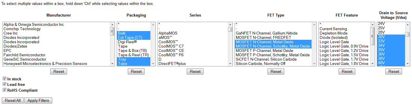
Using the above criteria, it is quite easy to use the filtering functions of e.g. Digikey to find a bunch of suitable transistors. Here is how I would do it on Digikey:
Go to their front page and click on Product Index.
Under the heading “Discrete Semiconductor Products”, click on “FETs – single“.
Hold down the Ctrl key and click on Bulk, Cut Tape, Tray and Tube in the Packaging box. This eliminates some uninteresting (for us) packaging alternatives.
In the FET Type box, select “MOSFET N-Channel, Metal Oxide” and “MOSFET N-Channel, Schottky, Metal Oxide”.
In the Drain to Source Voltage box, click on 30V, hold down shift and click on 100V to select parts with this range of VDS. Parts outside this range is probably not of interest as they do either not fulfill our requirements or are highly overspecified and thus probably more expensive and/or worse in some other regard.
Tick the three boxes “In stock”, “Lead free” and “RoHS compliant.
The relevant part of the page should now look something like this:
Filtering of Digikey parts.
Click “Apply filters”.
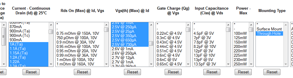
Still there are more than 3000 matches, so it would be nice to narrow the search further.
Select IDS between 1A and e.g. 30A (click on 1A, scroll to 30A, hold down shift and click on the 30A line)
Select VGS(th) between the minimum available and 2.5 V.
Select Through Hole in the Mounting Type box.
Now the selection should look like this:
Click Apply Filters again.
Currently, this results in only 20 hits for me and now it is time to look through the alternatives.
I do this by sorting on price, lowest first, by clicking on the up-arrow in the Price column.
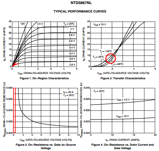
The first hit for me is a transistor called NTD5867 and looking at its datasheet it looks almost OK for this application. Below are some relevant plots. We can see that typically, a VGS of 2.8 V leads to a voltage drop of 0.5 V when the drain current is 2.5 A. For our currents which is about an order of magnitude smaller, the voltage drop should be negligible compared to the 12 V of the supply.
Some relevant plots from the datasheet of NTD5867.
These are however typical plots and we are not guaranteed that the transistor will work like this. The VGS(th) specification in the “Electrical characteristics” table says that VGS(th) is typically 1.8 V (at 250 µA and 25 °C), but that it can be as high as 2.5 V. This difference of 0.7 V means that we might need 3.5 V to achieve the behavior of the 2.8 V curve in the first plot above. And we do not have 3.5 V available to drive the transistor.
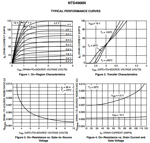
The second part in the Digikey results is NTD4906. Digikey says that this transistor has a VGS(th) of at most 2.2 V (compared to 2.5 V of the part above). Looking into the datasheet reveals a few other positive things, namely that that the difference between typical and maximum VGS(th) is 0.6 V and that it can conduct much more current at much less voltage drop at lower VGS than the previous part we looked at. Here are the plots for NTD4906:
Some relevant plots from the datasheet of NTD4906.
At 2.4 V VGS it can typically conduct about 2 A with a voltage drop of 0.5 V, so if we add the 0.6 V difference between typical and maximum VGS(th), we get this performance at 3 V gate-source drive, which the R Pi can provide.
Based on the above, I would recommend NTD4906N as the transistor to use for this purpose, although there are of course many others that would fit the bill. If you are not shopping at Digikey, you can use the same criteria to try to find another suitable transistor that is available to you.
DC/DC PMOS Transistor
The process of finding a suitable PMOS transistor for the DC/DC converter is very similar to what I described above. Here the criteria are primarily: at least 2 A drain current, at least 30 V drain-source voltage and besides that we want good efficiency and thus prefer low gate charge/gate capacitance and an on-resistance that is low compared to the 0.27 Ω current sense resistor. Threshold voltage is not an issue here as we are driving the transistor with pretty much the full input voltage of nominally 12 V, but it is important that the transistor can tolerate this gate-source voltage.
After narrowing down the search criteria, the transistor FQU11P06 shows up and its datasheet shows no obvious drawbacks. It has an on-resistance of at most 0.185 Ω at 10 V gate-source voltage and a gate charge of 17 nC.
There are a few other and somewhat more expensive parts that have lower on-resistance and less gate charge, like STF10P6F6, but the minor efficiency improvement is probably not worth the higher price in this case. So FQU11P06 would be my recommendation in this case.
Shutter/Focus Transistor
Here we need a small-signal NMOS transistor with criteria very similar to the NMOS transistor for the motor drive, except that we do not need nearly as much current carrying capability. Oddly enough the selection of hole-mounted small-signal NMOS transistors turn out to be not that great. The part that I think looks best at Digikey is ZVNL110A.
The funny thing is that it is more expensive ($0.78) than the bigger NTD4906N ($0.57) we selected above, so if you do not mind the size, you could actually use NTD4906N here as well.
If you are OK with using a surface mount transistor, there are more options. BSS123 is widely available and seems to fit the bill, although there may be variations in the threshold voltage limits from different manufacturers, so check the datasheet for the part you are about to buy.
DC/DC Inductor
The requirements on the inductor are primarily that the inductance shall be at least 220 µH and that the DC resistance shall be low to keep the efficiency high. And also that it shall be able to support enough peak current, which is probably around 1.5 A or so. The inductor I used has a resistance of 0.13 Ω, so this is a value to aim for to get the same or better efficiency.
Digikey does of course have a number of inductors that would do the job, but the one that seems to be least expensive is 2116-H-RC from Bourns. It is a toroid that has an inductance of 220 µH, a maximum current of 2.4 A and a maximum DC resistance of 0.12 Ω.
I hope the information in this blog post makes it easier to find suitable components for this project.
In my previous blog post about the inductance of some decoupling layouts, I concluded that using two 0402 capacitors would (almost) always be a better choice than using one 0306 capacitor. Andrew commented that mutual inductance might have an effect and he wanted to see measurements of layouts where two 0402 capacitors were present. Fortunately, my test layout supports that and I have now made a few extra measurements to see how two 0402s in parallel actually performs.
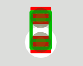
Here is a picture of the top side of the layout with the relevant components in color. For more details about the layout see the previous blog post.
Top view of the layout, including the shape of the power plane. Footprints not discussed in this blog post are grayed out.
The new combinations I tested were capacitors on:
C110 and C117; two 0402s close to each other (but connected in reverse) taking up roughly the same area as one 0306.
C110 and C112; two 0402s far from each other and thus without inductive coupling.
The same cases as above but on the bottom side of the PCB and thus further from the planes.
I also include old data for the 0306 at position C132 for comparison as well as data for the single 0402 at C112.
Case 1 might give some inductive coupling between the components and vias, especially on the bottom side where the vias are longer and the capacitors are further from the planes. The coupling should help reduce the inductance since the currents in the nearby capacitors and vias flow in opposite directions.
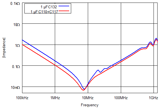
Here is an impedance plot comparing the impedance of one 0306 to that of two 0402s on the top side of the board.
Impedance of a 0306 capacitor (blue) compared to impedance of dual 0402 capacitors (red).
The dual 0402 is the winner since it has lower impedance for all frequencies. The reason it has lower impedance at low frequencies is that the combination has higher capacitance. Interestingly though, it does not quite have twice the capacitance of a single 1 µF 0306. (In my experience, 1 µF 0402 capacitors are always a bit below 1 µF and they are also much more voltage dependent than 1 µF capacitors in larger packages. So do not count on getting 1 µF of capacitance from an 0402 capacitor, especially not if you have some voltage across it.)
Below is the table with the results of the measurements. Layouts E and G were presented in the previous blog post whereas I and J are new.
E
G
Layout
Desc
0402
via in pad
0.3/0.6 mm vias
C/C = 0.7 mm
0306
via in pad
0.3/0.6 mm vias
C/C = 0.7 mm
Top
0.44 nH
0.28 nH
Bottom
1.04 nH
0.62 nH
I
J
Layout
Desc
Dual 0402
close together
via in pad
0.3/0.6 mm vias
C/C = 0.7 mm
Dual 0402
far away
via in pad
0.3/0.6 mm vias
C/C = 0.7 mm
Top
0.24 nH
0.21 nH
Bottom
0.51 nH
0.51 nH
Observations
In both cases of dual 0402 layouts, the inductance was less than the inductance of the best 0306 layout, just as predicted.
The two 0402 that were placed close together had a slightly higher inductance on the top side than the other variant, despite the inductive coupling that should help reduce the inductance. Maybe this is measurement error or maybe the result is caused by differences in plane imperfections (anti-pads) close to the capacitors. Or perhaps it is the result of that the current going to both capacitors flows in the same part of the planes, whereas current flows in different parts of the planes when the capacitors are far away so that the plane inductances appear in parallel.
If the latter is the main reason for the difference in top side inductance, the fact that the bottom side inductances came out the same might be explained by the additional plane inductance being offset by the reduction in inductance caused by the inductive coupling between the (long) vias and the components that are far from the planes. The inductive coupling is likely to have a bigger effect on the bottom side since the vias are longer and the capacitors are further from the planes.
So, the prediction from the previous blog post that using 0402s is a better idea than using half as many 0306s holds up well.