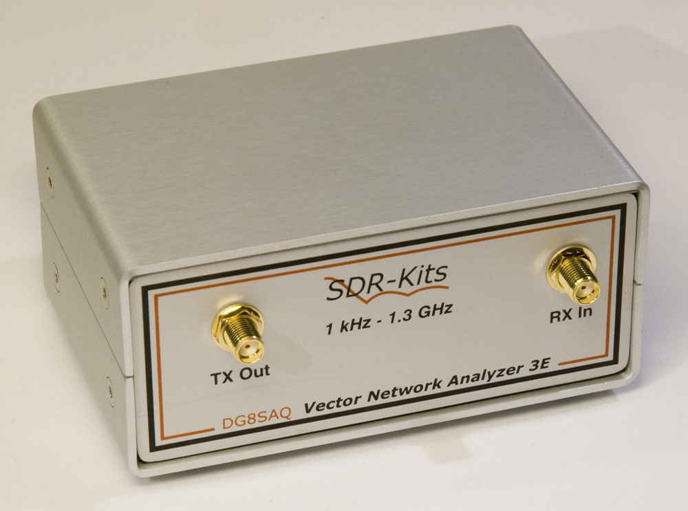
I bought myself a somewhat unusual Christmas present a few weeks ago, namely a vector network analyzer, VNA. All VNAs I had previously used were huge and very expensive instruments, but it turns out that there is an interesting alternative out there on the market. Tom Baier, a radio amateur with the call sign DG8SAQ has created a really neat product he calls the “VNWA 3E“. It is a VNA in a small box powered via USB and controlled by a PC.
(I do not know why everybody insist on using the abbreviation VNWA instead of VNA for this particular VNA, but it seems like VNWA has become the accepted name for this device, so I will use it when referring to this product and not VNAs in general.)
Technical description
The VNWA design itself is very clever as it covers a relatively large frequency range while still being orders of magnitude cheaper than traditional VNAs. It achieves this through a minimalistic design and a combination of using harmonic overtones of the frequency synthesizers, overclocking the synthesizers outside of their specified frequency range and also using mixers outside of their specified operating range. The main downside of this approach seems to be that the dynamic range suffers for frequencies above 500 MHz. Also, the maximum output power is really low at -17 dBm at 1 MHz and less for higher frequencies. This however is usually not a major problem.
AD9859 10-bit DDS (direct digital synthesis) chips are used for both the RF and the LO oscillators. These are specified for clock frequencies of up to 400 MHz, so normally they could only be used to generate signals up to a bit below 200 MHz. But it turns out they always seem to work fine when overclocked up to 720 MHz, and by utilizing harmonics, much higher frequencies can be probed than one would originally expect.
An IF of between 1 kHz and 12 kHz is used and it is sampled by an audio ADC. There does not seem to be any explicit IF filter in the design and one can in particular not select between different IF bandwidths as is possible on most other VNAs. It is however possible to select the measurement time at each frequency point.
The VNWA 3E can measure both S11 and S21 (reflected and through) S-parameters at the same time since it contains an expansion board with an extra audio ADC. To measure S22 and S12 (reflection from output and reverse transmission) the connections to the device under test (DUT) have to be manually swapped.
Below is a partial block diagram of an earlier version of the VNWA where a PC soundcard was used as the sampler of the IF and reference signals.
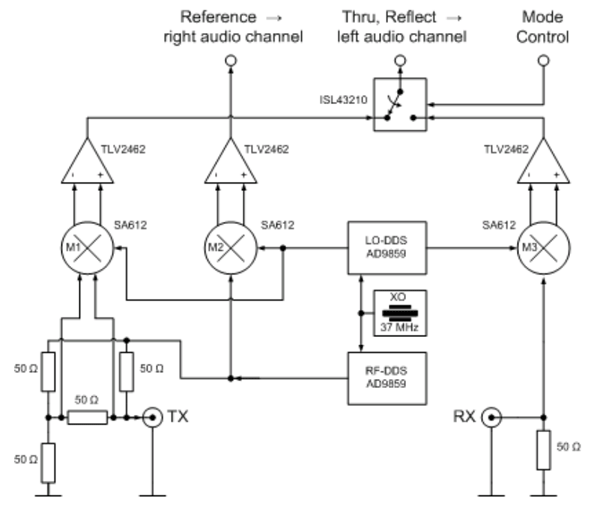
Due to the shortcuts taken in the design of the VNWA, there are thus some shortcomings and a few features missing that one would find in a traditional VNA, but there are also many useful features provided in the software that I have not seen in other VNAs. Considering the price, I think the instrument is a bargain if you want to make measurements in the 200 Hz to 1.3 GHz range and can live with a dynamic range of about 50 dB above 500 MHz.
Whistling inductor
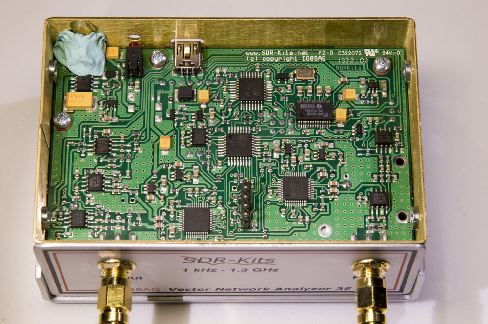
When I received the VNWA, I was first struck by its small size. I had expected it to be small, but not so small. It is only 10.4 cm wide. The installation went fine, but there was an audible whistling noise coming from the device. It sounded like noise I had previously heard from some DC/DC-converters. I contacted SDR-kits where I bought the VNWA and was told that the noise problem could be solved by putting a drop of glue on top of the inductor of a DC/DC converter.
I took the unit apart (which is very simple to do) and put some hot melt glue on the suspect inductor, glueing it to the side wall. On top of that I put some Tack-It. This largely eliminated the noise, although I can still hear it if I listen close to the device. Looking at the circuitry around the inductor, it is apparent that a MAX632 is used as a step-up converter and this chip seems both expensive and outdated. It switches at 45 kHz and the regulation is done by skipping cycles, rather than by adjusting the duty cycle. This probably leads to the ripple current having lots of frequency content in the audible spectrum, which the inductor converts to sound. A more modern step-up-regulator would probably both reduce the cost and get rid of the noise. Below is a photo showing the inductor covered in glue and Tack-It.
Some tests
To try out my new toy, I did a couple of measurements. First I tested three different attenuators.
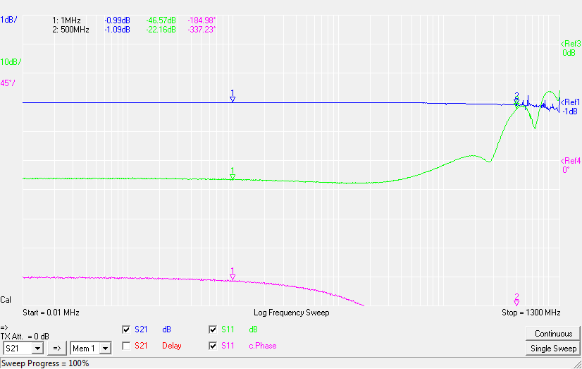
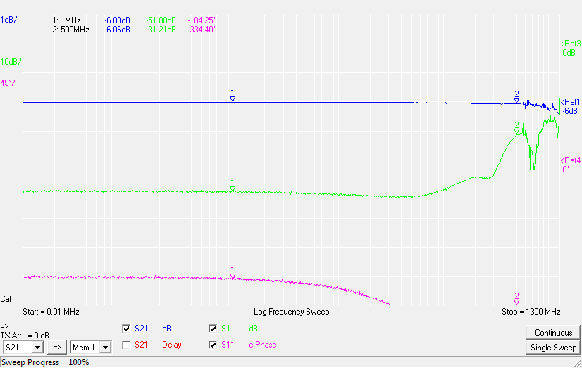
All of these three attenuators are specified to have about 0.2 dB excess loss at 1 GHz. This is approximately what the VNWA shows for the 1 and 6 dB attenuators, but it looks more like 0.4 dB extra loss for the 20 dB attenuator. Also, the S21 (transmission) curve looks a little jagged above 500 MHz, which is probably the decreased sensitivity and accuracy in this frequency range showing up.
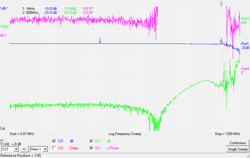
Next I tried a 90 MHz low-pass filter. Comparing this to the datasheet, it seems like the filter has less loss at 90 MHz than what is typical. The 3 dB frequency is actually 95.8 MHz. VSWR in the pass band is also better than typical (< 1.42 whereas the DS says < 1.7). The stopband attenuation should be greater than 70 dB between 230 and 400 MHz, and this is also shown by the VNWA. The datasheet gives no data above 400 MHz and I do not trust the VNWA to say much about attenuations larger than 50 dB above 500 MHz.
Component measurements
One of the great things with a VNA is that it can be used to measure component parameters over a range of frequencies. It can therefore be used to measure e.g. inductance and capacitance. The VNWA actually has a built-in LCR-meter function measuring at a single (but selectable) frequency, but I prefer to do a sweep and see how the measured value changes with frequency. In that way it becomes obvious if the component that is tested behaves in the expected manner (like a capacitor keeping its capacitance over a range of frequencies).
There are different ways to use a VNA to measure impedance. Basically, one can base the measurements on reflected waves (S11) or transmitted waves (S21). The S11 method has the advantage that only one cable is needed, while the S21 method requires two cables, but has advantages in terms of easier calibration and more precise results when the impedance is very high or very low compared to the system impedance of 50 ohms. When doing S21 impedance measurements, the unknown impedance can either be placed in series with the signal path (good for high impedances) or shunting the signal to ground (good for low impedances).
The VNWA software has built-in support to convert S11-data to capacitance and inductance but does not seem to have direct support for the S21 methods of component measurements. A great feature though is that it is possible to define custom formulas that do the conversion from S-parameters to e.g. capacitance or inductance, so the results of S21-based component measurements can be easily plotted.
I tested a few different components using an educational test fixture I bought together with the VNA and seemed to get good results. Below is a picture of the VNWA with the test fixture in front.
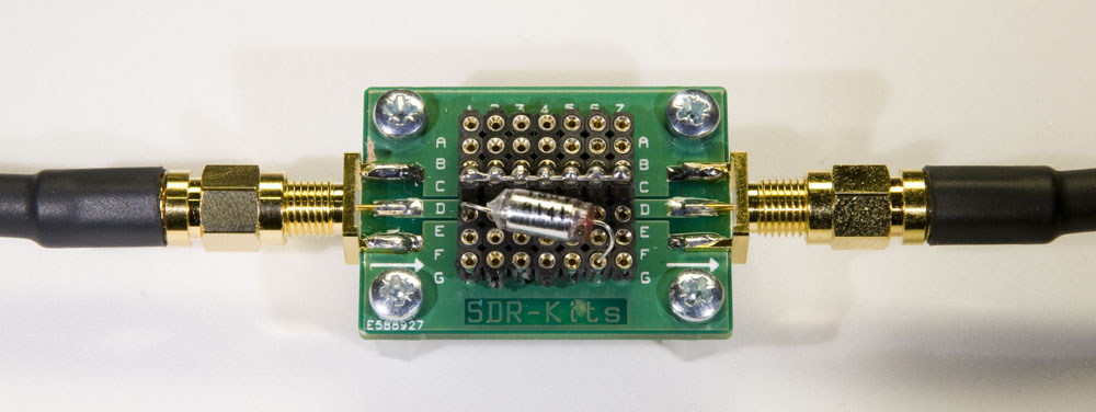
Clearly, the fixture is not designed to have low parasitics at high frequencies, but it should be useful up to at least a few MHz.
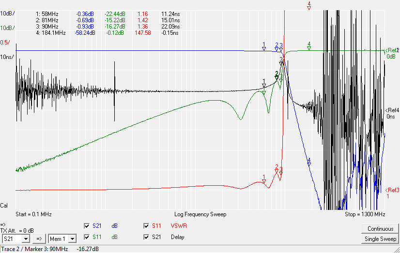
First I tested two inductors, one that I found in a DC/DC converter I discussed in a previous blog post and a random toroid I had in the junk bin.
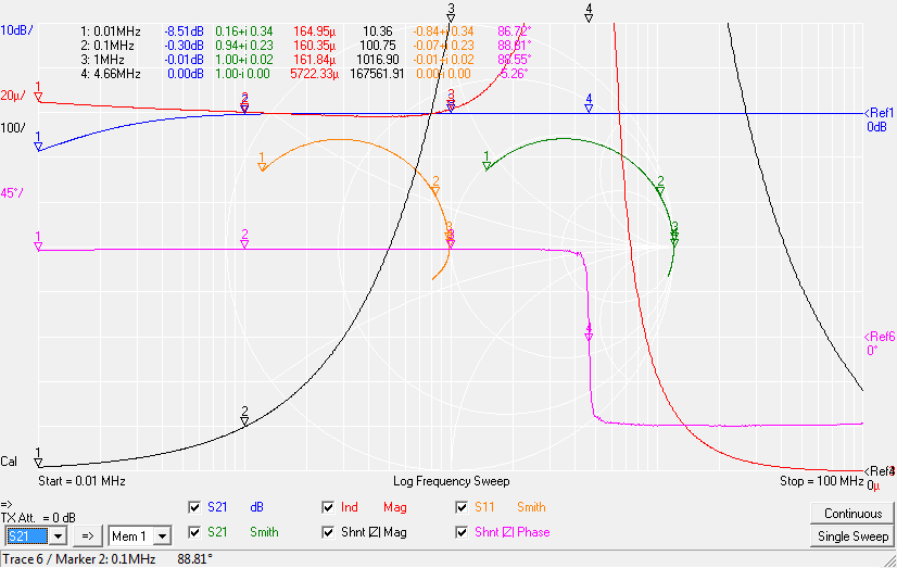
I connected the inductor from the signal to ground, shunting the transmitted signal. Six different curves are plotted simultaneously:
- S21 is plotted both as magnitude and in a Smith chart,
- the inductance calculated from the S21-parameter,
- the magnitude of the shunting impedance (unfortunately it is not possible to use a logarithmic Y-axis when plotting, unless you plot dB),
- S11 in a Smith chart and
- the phase of the shunting impedance.
The reference levels and values can be seen at the right side of the plot while the per-division values can be seen on the left.
The calculated inductance drops slowly over the frequency range from 10 kHz (165 µH) via 100 kHz (160 µH) to 400 kHz before it approaches resonance at 4.7 MHz. The phase of the shunting impedance is close to 90 degrees up to 2-3 MHz. The inductance seems to be around 160 µH based on this test.
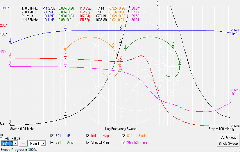
The toroid gave the below plot. The inductance is dropping from 10 kHz (114 µH) to 1 MHz (108 µH) where the phase is 70 degrees, indicating quite a bit of loss. This inductor has much more loss at higher frequencies than the previous one and is perhaps intended as a choke rather than as a low-loss inductor for e.g. a DC/DC converter.
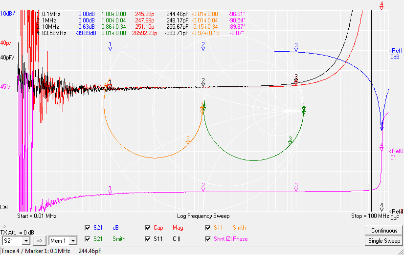
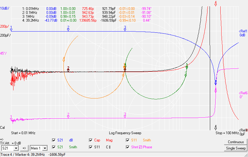
I also had a few low-tolerance capacitors and it seemed like a good idea to check what readings the VNWA would give when presented with these.
The first one is marked 246 pF 0.5%, so it should have a capacitance between 244.8 and 247.2 pF. I have plotted not only the capacitance calculated using my S21-based formula, but also the built-in S11-based formula. Both formulas give realistic values at the flat portion of the graphs with 247.7 pF for S21 and 248.2 pF for S11 at 1 MHz. A little smoothing would have been appropriate to get better readings at lower frequencies, although neither measurement method is suitable for measuring 246 pF below 100 kHz. Putting the capacitor in series would have given better LF-results for the S21 approach.
The second capacitor is marked 942 pF +/- 0.3% (thus 939.2 to 944.8 pF). A handheld component tester measured this as 944 pF. The S21 approach gives values within the tolerance range for both 100 kHz and 1 MHz, whereas the S11 approach is a little more variable.
The next capacitor is marked 10 nF +/- 0.5% (thus 9.95 to 10.05 nF). S21 gives values within this range for both 100 kHz and 500 kHz.
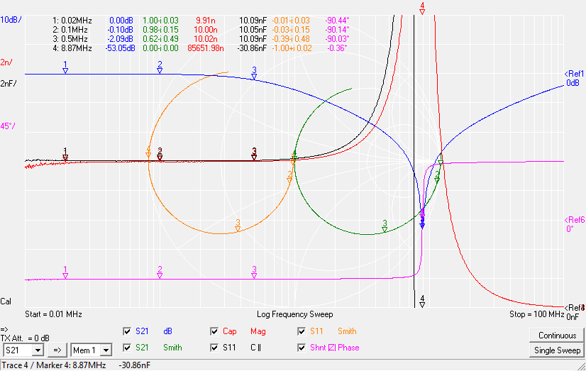
So in all, it seems like the VNWA is pretty useful to measure capacitances and inductances like these. The tolerance is probably better than 1% if the calibration and the measurements are made carefully.
A great Christmas present!
What made you select the VNWA-3E over other home built constructions (miniVNA for instance) and commercial models?
Hi Marcus,
I do not think I was aware of the miniVNA when I bought the VNWA, but even if I had been, I probably would have chosen the VNWA since I do want to be able to make measurements at really low frequencies. The miniVNA models only go down to 100 kHz or 1 MHz while the VNWA can be used down to about 200 Hz.
Commercial models from companies like HP/Agilent/Keysight, R&S, Anritsu or even Copper Mountain were outside of my budget.
Another nice thing about the VNWA is that there is a pretty active community around it (the mailing list VNWA@yahoogroups.com) and that the designer behind it, Tom Baier, is quite responsive and releases new software version regularly. The software is really good and well documented, although it might at first not be obvious how to use it or what features it contains.
Per