In 2008 I made a test board and did a series of network analyzer measurements to determine the effect of the layout on the inductance of decoupling (bypassing) capacitors on a multi-layer PCB. The results were published in Elektroniktidningen and on axotron.se (in Swedish, although the table with the important results is probably possible to understand even if you cannot read Swedish).
I have now built and tested a new test board with a new set of decoupling capacitor layouts and this time the layout includes both via-in-pad and reverse geometry (broadside) 0306 capacitors as well as normal 0402 capacitors. This blog post describes the new results.
A New Test Board
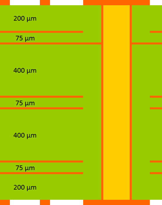
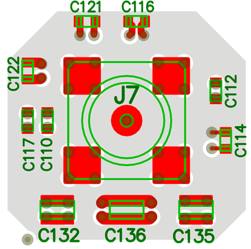
The new test layout resides on a corner of an 8-layer board. It consists of identical layouts on the top and bottom while the power plane is located much closer to the top than to the bottom. In this way, the effect of via length can be tested.
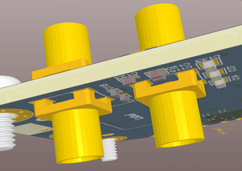
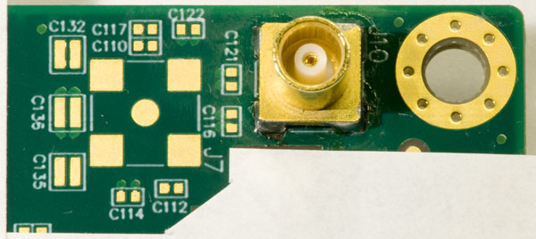
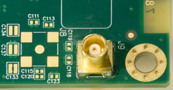
There is a surface mount coaxial MCX-connector on the top of the board and right under it is another MCX-connector. The signal pins of the two connectors are connected through a via that also connects to a minimal power plane inside the board. The ground pins sit on top of several vias that connect to the ground plane inside the board. Overplated via technology is used, so it is allowed to put vias directly in the pads of the components without any risk of solder being sucked away from the pads.
There is also another pair of MCX-connectors on the board. They are identically connected, except that the signal via goes straight through the PCB without connecting to any plane. This is for performing the thru calibration of the network analyzer (VNA). It allows the VNA to subtract out any parasitics and the delay associated with the connectors and vias so that only the effects of the plane and the capacitors are measured.
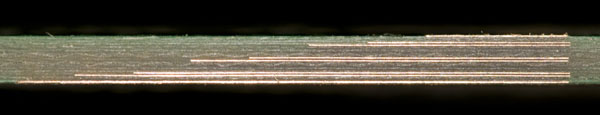
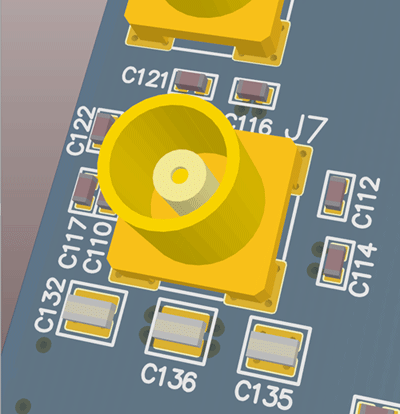
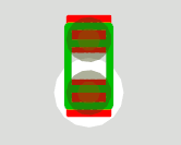
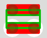
Below is a series of pictures illustrating the layout and stackup.
To measure the inductance, a vector network analyzer (VNA) is used. Theoretically, one could connect just one cable and measure S11 (essentially how much of the incoming wave is reflected back to the VNA) but this method is not so stable when measuring really low impedances (relative to 50 Ω) and calibration is also a problem, since one would like to measure the impedance right at the power plane. Therefore S21 is measured, i.e. how much of the incoming wave passes through to the other MCX connector. With this method it is easier to do the calibration and the results are much more reliable for impedances much lower than 50 Ω. The use of S21 is the reason for the two connectors on opposite sides of the board as well as the pair of thru calibration connectors.
It is straightforward to derive an expression for the shunting impedance as a function of the measured S21 value:
![]()
If the plane capacitance is small compared to the capacitance of the decoupling capacitor (and the parasitic inductance is not too small), there is a frequency range between the series resonance (of the capacitor) and the parallel resonance (between the plane capacitance and the inductance of the capacitor) where the inductance of the capacitor dominates. This is where it is easiest to deduce the inductance of the capacitor and its layout.
To further improve the inductance measurement, S21 of the plane was first measured and converted to shunting impedance. This impedance was then mathematically removed from the impedance of each capacitor/plane combination (by treating it as being in parallel with the capacitor impedance). This correction is small for frequencies below 100 MHz and only results in a few percent change in the calculated inductance. The effect on the impedance for a typical case is shown in the plot below.
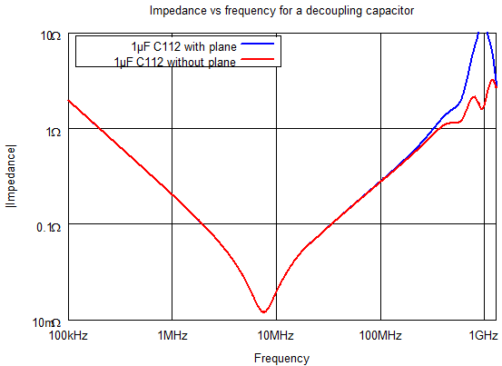
- Impedance vs frequency of a 1 µF 0402 capacitor at location C112. The impedance contributed by the plane has been mathematically removed in the red curve, but not in the blue.
Only one capacitor at a time was mounted on the board and then S21 was measured. This allowed calculation of the inductance of each of the different decoupling layout variants. The frequency 100 MHz was chosen as the point where the inductance was evaluated. The reason for this is that it is close to the geometric mean between the series and parallel resonances. It turns out that the inductance value one obtains is slightly dependent upon the selected frequency. The value decreases by about 4-8% from 30 MHz to 200 MHz, but this amount of uncertainty is probably smaller than the uncertainty caused by factors such as capacitor placement tolerance, board layer thickness variation and general measurement tolerance.
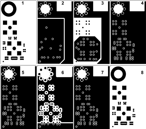
Below is the table with the results of the measurements. Eight different layouts were tested and the inductance was measured on both the top and the bottom side of the board.
| A | B | C | |
|---|---|---|---|
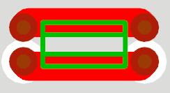
| Layout | 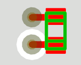 |
 |
 |
| Desc | 0402 W:0.2 L:0.8 mm tracks 0.3/0.6 mm vias C/C = 0.8 mm |
0402 W:0.35 L:0.8 mm tracks 0.3/0.6 mm vias C/C = 0.7 mm |
0402 W:0.35 L:0.83 mm tracks close together 0.3/0.6 mm vias C/C = 0.7 mm |
| Top | 0.63 nH | 0.60 nH | 0.56 nH |
| Bottom | 1.35 nH | 1.22 nH | 1.16 nH |
| D | E | F | |
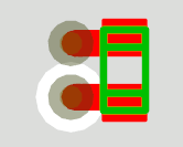
| Layout | 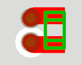 |
 |
 |
| Desc | 0402 W:0.5 L:0.8 mm tracks 0.3/0.6 mm vias C/C = 0.7 mm |
0402 via in pad 0.3/0.6 mm vias C/C = 0.7 mm |
0306 via in pad 0.3/0.6 mm vias C/C = 0.9 mm |
| Top | 0.59 nH | 0.44 nH | 0.29 nH |
| Bottom | 1.20 nH | 1.04 nH | 0.70 nH |
| G | H | ||
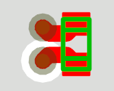
| Layout | 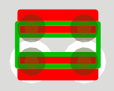 |
 |
|
| Desc | 0306 via in pad 0.3/0.6 mm vias C/C = 0.7 mm |
0306 0.6 mm tracks 0.3/0.6 mm vias C/C = 0.7 mm |
|
| Top | 0.28 nH | 0.30 nH | |
| Bottom | 0.62 nH | 0.64 nH | |
Observations
- Layout A is similar to Layout H in the tests I did in 2008, which showed 0.78 nH/1.05 nH top/bottom inductance. The new layout shows lower inductance for the top side, but higher for the bottom side, despite the similarities. The different results may be the result of subtle differences in the test boards. The most important ones are that the previous test board had ground planes on layers 4-7 in addition to the main ground plane on layer 2 and that the previous test board had 0.2 mm spacing between all layers, whereas the new board has 0.075 mm spacing within the power/ground plane pair. The smaller plane separation means that the power plane is closer to the top (lower inductance on the top side and higher on the bottom side) and the additional ground planes on the previous test board provides additional paths for the ground current through the other ground vias and that reduces the inductance. These layout differences might account for the differences in inductance.
- Layout B is slightly better than layout A as expected due to the wider traces. The effect is small but worth while since wider traces do not cost extra. The improvement might in fact be partly obscured by a somewhat unfortunate layout. The power plane close to the power via of C121 has more holes cut in it than around C114. The extra holes increase the inductance.
- Layout C shows that keeping the tracks closer together might give a small advantage. This layout (C116) is less affected by MCX ground vias than C121, so at least part of the improvement over layout B might be attributable to the more solid power plane close to the power via.
- Layout D with even wider traces than layout B gives a (very) small improvement. This layout is also affected by nearby holes in the power plane and one can perhaps not conclude that layout C is better than layout D because of this.
- Layout E shows the effect of using (overplated) via-in-pad. The result is significantly better than the previous layouts, especially for the bottom side. Less than 0.5 nH inductance on the top side and 1 nH for a capacitor on the bottom side is really good.
- In layout F, a more exotic reverse geometry 0306 capacitor is used together with via-in-pad. At first it looks really good with 0.3 nH on the top side and 0.7 nH on the bottom, but this layout has four vias instead of two and uses a more expensive part, so perhaps it should rather be compared with using two 0402 capacitors and then its performance is no longer outstanding.
- Layout G shows the effect of bringing the vias closer together. This has the most effect on the bottom sides where the current flows through a longer section of the vias.
- Layout H shows an 0306 used without via-in-pad. This does not give a significant penalty, so the benefit of via-in-pad is not dramatic when using 0306 components.
0306 vs 0402
Is it worth while using reverse geometry 0306 capacitors instead of ordinary 0402s?
My conclusion is that using 0306 capacitors is rarely if ever a better choice. In all the 0306 cases tested here, the inductance was more than half the inductance of a corresponding 0402 layout, so by using two 0402s (which have the same number of vias and take up roughly the same area), the same or better results can be achieved. The 0402 alternative gives more layout flexibility in tight layouts since they can be placed separately in two smaller free areas, like in the middle of a 1 mm pitch via array under a BGA package (utilizing via-in-pad or suitable octagonal SMD pads).
From a cost perspective it looks like 0306 also comes out short. A 1 µF, 10 V, 0402 with X5R dielectric currently costs about $0.011 at Digikey in quantities of 1000. The least expensive 1 µF, 10 V, 0306, X5R capacitor that Digikey currently stocks costs $0.13 in quantities of 1000, but they also list a 1 µF, 10V, 0306, X7R capacitor for $0.043. A few of them are in stock as I write this, but it is not generally stocked. It is however stocked at Mouser for $0.052 in quantities of 1000. So it seems like one 0306 costs at least twice as much as two 0402. The assembly cost can vary widely, but $0.01 per capacitor might be in the right ball park. In that case the total cost difference between one 0306 and two 0402 becomes smaller, but still hardly to the advantage of 0306.
If you need high decoupling capacitance and operation above 85 °C, X5R dielectrics is not good enough and X7R or X7S (or better) should be used. Digikey has 0.68 µF, 6.3 V, 0402, X7S capacitors that cost $0.021 @1000. So with these requirements 0306 and 0402 might be more or less equivalent from a cost perspective.
So typically it seems like a better idea to stick with traditional 0402 capacitors (and use twice as many) than to use 0306 since it gives better performance, lower cost and higher layout flexibility.
Conclusions
- Using (overplated) via-in-pad technology can give a 15-30% reduction in decoupling inductance for 0402 capacitors.
- The improvement is largest when the planes are close to the capacitor, i.e. when via inductance is a smaller part of the total parasitic inductance.
- Using 0306 capacitors gives lower inductance per capacitor (than using 0402 capacitors), but does typically not give lower inductance per via used, per $ spent or per board area used for decoupling.
- In the majority of cases it is better to use 0402 decoupling capacitors than to use half as many 0306 capacitors.
Update: To test whether dual 0402s are actually better than a single 0306, I did some more measurements and wrote about them in a new blog post.
It’s not exactly fair to say that two 0402’s in parallel will have half the inductance, since there will be mutual inductance between the two current paths in addition to the self inductance of each capacitor. It’d be interesting to see a direct comparison with a pair of 0402’s.
Thanks for you comment Andrew. My layout accommodates the additional tests you suggest, so I did the measurements and wrote a new post about them: http://axotron.se/blog/more-decoupling-layout-inductance-measurements/
The result is that two 0402s do indeed give lower inductance than one 0306, both when the capacitors are close to each other and when they are far away.
I have some question about the through calibration. How the through calibration is done to subtract out any parasitics and the delay associated with the connectors and vias?
Hi Shane,
The board has a pair of calibration connectors, J9 and J10 as shown in the photos. They are located on opposite sides of the board right on top of each other, just like the measurement connectors. The pair of calibration connectors is identical to the pair of measurement connectors, except that the signal pins of the calibration connectors are not connected to the power plane, only to each other.
To calibrate, I just connect the cables to the calibration connectors and do a through calibration.
The only difference between the calibration circuit and the tested circuit is the fact that there is a plane with a decoupling capacitor shunting the signal between the test connectors. Therefore everything except this shunting impedance is calibrated out, which is exactly what one wants.
Per