Inductance of some Decoupling Layouts

In 2008 I made a test board and did a series of network analyzer measurements to determine the effect of the layout on the inductance of decoupling (bypassing) capacitors on a multi-layer PCB. The results were published in Elektroniktidningen and on axotron.se (in Swedish, although the table with the important results is probably possible to understand even if you cannot read Swedish).

I have now built and tested a new test board with a new set of decoupling capacitor layouts and this time the layout includes both via-in-pad and reverse geometry (broadside) 0306 capacitors as well as normal 0402 capacitors. This blog post describes the new results.

A New Test Board

The new test layout resides on a corner of an 8-layer board. It consists of identical layouts on the top and bottom while the power plane is located much closer to the top than to the bottom. In this way, the effect of via length can be tested.

There is a surface mount coaxial MCX-connector on the top of the board and right under it is another MCX-connector. The signal pins of the two connectors are connected through a via that also connects to a minimal power plane inside the board. The ground pins sit on top of several vias that connect to the ground plane inside the board. Overplated via technology is used, so it is allowed to put vias directly in the pads of the components without any risk of solder being sucked away from the pads.

There is also another pair of MCX-connectors on the board. They are identically connected, except that the signal via goes straight through the PCB without connecting to any plane. This is for performing the thru calibration of the network analyzer (VNA). It allows the VNA to subtract out any parasitics and the delay associated with the connectors and vias so that only the effects of the plane and the capacitors are measured.

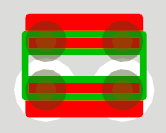
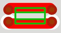
Below is a series of pictures illustrating the layout and stackup.
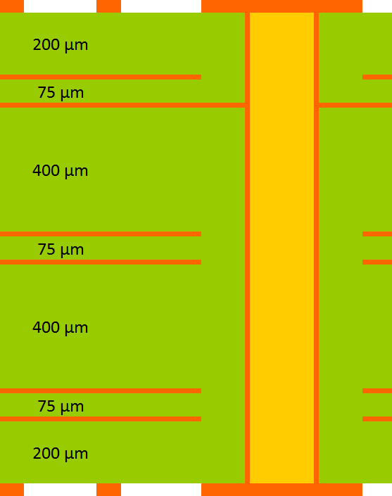
Stackup of the 8-layer test board
Stackup of the 8-layer test board. The distance between the power and the ground planes is nominally 75 µm. The distance from the power plane to the top is ~300 µm and the distance from the power plane to the bottom is 1200 µm.
Photo of a cross section of the PCB showing the copper layers.
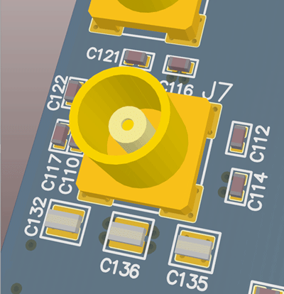
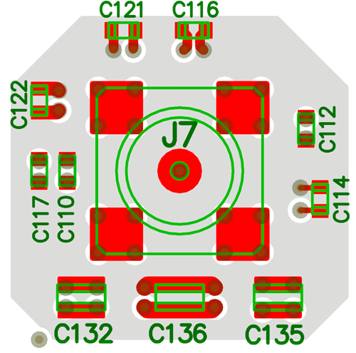
3D view of the top side of the layout
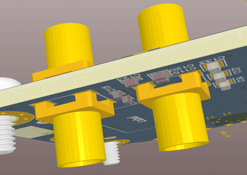
3D side view of the layout
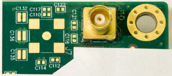
Top side of PCB (with calibration connector)
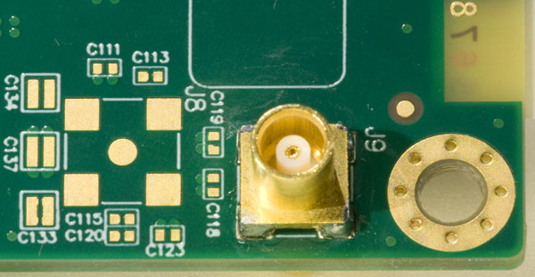
Bottom side of PCB (with calibration connector)
Top view of the layout, including the shape of the power plane.
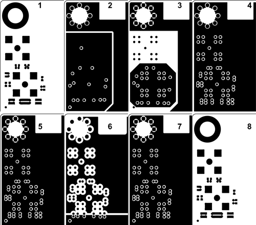
The layout on each of the eight copper layers. Layer 2 is the ground plane and layer 3 is the power plane. The other inner layers are not connected to the test circuitry.

To measure the inductance, a vector network analyzer (VNA) is used. Theoretically, one could connect just one cable and measure S11 (essentially how much of the incoming wave is reflected back to the VNA) but this method is not so stable when measuring really low impedances (relative to 50 Ω) and calibration is also a problem, since one would like to measure the impedance right at the power plane. Therefore S21 is measured, i.e. how much of the incoming wave passes through to the other MCX connector. With this method it is easier to do the calibration and the results are much more reliable for impedances much lower than 50 Ω. The use of S21 is the reason for the two connectors on opposite sides of the board as well as the pair of thru calibration connectors.

It is straightforward to derive an expression for the shunting impedance as a function of the measured S21 value:

Z_S21
If the plane capacitance is small compared to the capacitance of the decoupling capacitor (and the parasitic inductance is not too small), there is a frequency range between the series resonance (of the capacitor) and the parallel resonance (between the plane capacitance and the inductance of the capacitor) where the inductance  of the capacitor dominates. This is where it is easiest to deduce the inductance of the capacitor and its layout.

To further improve the inductance measurement, S21 of the plane was first measured and converted to shunting impedance. This impedance was then mathematically removed from the impedance of each capacitor/plane combination (by treating it as being in parallel with the capacitor impedance). This correction is small for frequencies below 100 MHz and only results in a few percent change in the calculated inductance. The effect on the impedance for a typical case is shown in the plot below.
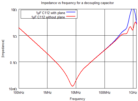
Impedance vs frequency of a 1 µF 0402 capacitor at location C112 (the impedance contributed by the plane has been mathematically removed in the red curve, but not in the blue).

Impedance vs frequency of a 1 µF 0402 capacitor at location C112. The impedance contributed by the plane has been mathematically removed in the red curve, but not in the blue.

Only one capacitor at a time was mounted on the board and then S21 was measured. This allowed calculation of the inductance of each of the different decoupling layout variants. The frequency 100 MHz was chosen as the point where the inductance was evaluated. The reason for this is that it is close to the geometric mean between the  series and parallel resonances. It turns out that the inductance value one obtains is slightly dependent upon the selected frequency. The value decreases by about 4-8% from 30 MHz to 200 MHz, but this amount of uncertainty is probably smaller than the uncertainty caused by factors such as capacitor placement tolerance, board layer thickness variation and general measurement tolerance.

Below is the table with the results of the measurements. Eight different layouts were tested and the inductance was measured on both the top and the bottom side of the board.

A B C
Layout
Desc 0402
W:0.2 L:0.8 mm tracks
0.3/0.6 mm vias
C/C = 0.8 mm
0402
W:0.35 L:0.8 mm tracks
0.3/0.6 mm vias
C/C = 0.7 mm
0402
W:0.35 L:0.83 mm tracks
close together
0.3/0.6 mm vias
C/C = 0.7 mm
Top 0.63 nH 0.60 nH 0.56 nH
Bottom 1.35 nH 1.22 nH 1.16 nH
D E F
Layout
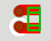
Desc 0402
W:0.5 L:0.8 mm tracks
0.3/0.6 mm vias
C/C = 0.7 mm
0402
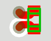
via in pad
0.3/0.6 mm vias
C/C = 0.7 mm
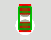
0306
via in pad
0.3/0.6 mm vias
C/C = 0.9 mm
Top 0.59 nH 0.44 nH 0.29 nH
Bottom 1.20 nH 1.04 nH 0.70 nH
G H
Layout
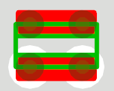
Desc 0306
via in pad
0.3/0.6 mm vias
C/C = 0.7 mm
0306
0.6 mm tracks
0.3/0.6 mm vias
C/C = 0.7 mm
Top 0.28 nH 0.30 nH
Bottom 0.62 nH 0.64 nH

Observations

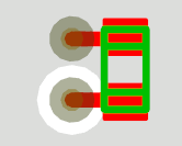
  • Layout A is similar to Layout H in the tests I did in 2008, which showed 0.78 nH/1.05 nH top/bottom inductance. The new layout shows lower inductance for the top side, but higher for the bottom side, despite the similarities. The different results may be the result of subtle differences in the test boards. The most important ones are that the previous test board had ground planes on layers 4-7 in addition to the main ground plane on layer 2 and that the previous test board had 0.2 mm spacing between all layers, whereas the new board has 0.075 mm spacing within the power/ground plane pair. The smaller plane separation means that the power plane is closer to the top (lower inductance on the top side and higher on the bottom side) and the additional ground planes on the previous test board provides additional paths for the ground current through the other ground vias and that reduces the inductance. These layout differences might account for the differences in inductance.
  • Layout B is slightly better than layout A as expected due to the wider traces. The effect is small but worth while since wider traces do not cost extra. The improvement might in fact be partly obscured by a somewhat unfortunate layout. The power plane close to the power via of  C121 has more holes cut in it than around C114. The extra holes increase the inductance.
  • Layout C shows that keeping the tracks closer together might give a small advantage. This layout (C116) is less affected by MCX ground vias than C121, so at least part of the improvement over layout B might be attributable to the more solid power plane close to the power via.
  • Layout D with even wider traces than layout B gives a (very) small improvement. This layout is also affected by nearby holes in the power plane and one can perhaps not conclude that layout C is better than layout D because of this.
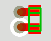
  • Layout E shows the effect of using (overplated) via-in-pad. The result is significantly better than the previous layouts, especially for the bottom side. Less than 0.5 nH inductance on the top side and 1 nH for a capacitor on the bottom side is really good.
  • In layout F, a more exotic reverse geometry 0306 capacitor is used together with via-in-pad. At first it looks really good with 0.3 nH on the top side and 0.7 nH on the bottom, but this layout has four vias instead of two and uses a more expensive part, so perhaps it should rather be compared with using two 0402 capacitors and then its performance is no longer outstanding.
  • Layout G shows the effect of bringing the vias closer together. This has the most effect on the bottom sides where the current flows through a longer section of the vias.
  • Layout H shows an 0306 used without via-in-pad. This does not give a significant penalty, so the benefit of via-in-pad is not dramatic when using 0306 components.

0306 vs 0402

Is it worth while using reverse geometry 0306 capacitors instead of ordinary 0402s?

My conclusion is that using 0306 capacitors is rarely if ever a better choice. In all the 0306 cases tested here, the inductance was more than half the inductance of a corresponding 0402 layout, so by using two 0402s (which have the same number of vias and take up roughly the same area), the same or better results can be achieved. The 0402 alternative gives more layout flexibility in tight layouts since they can be placed separately in two smaller free areas, like in the middle of a 1 mm pitch via array under a BGA package (utilizing via-in-pad or suitable octagonal SMD pads).

From a cost perspective it looks like 0306 also comes out short. A 1 µF, 10 V, 0402 with X5R dielectric currently costs about $0.011 at Digikey in quantities of 1000. The least expensive 1 µF, 10 V, 0306, X5R capacitor that Digikey currently stocks costs $0.13 in quantities of 1000, but they also list a 1 µF, 10V, 0306, X7R capacitor for $0.043. A few of them are in stock as I write this, but it is not generally stocked. It is however stocked at Mouser for $0.052 in quantities of 1000. So it seems like one 0306 costs at least twice as much as two 0402. The assembly cost can vary widely, but $0.01 per capacitor might be in the right ball park. In that case the total cost difference between one 0306 and two 0402 becomes smaller, but still hardly to the advantage of 0306.

If you need high decoupling capacitance and operation above 85 °C, X5R dielectrics is not good enough and X7R or X7S (or better) should be used. Digikey has 0.68 µF, 6.3 V, 0402, X7S capacitors that cost $0.021 @1000. So with these requirements 0306 and 0402 might be more or less equivalent from a cost perspective.

So typically it seems like a better idea to stick with traditional 0402 capacitors (and use twice as many) than to use 0306 since it gives better performance, lower cost and higher layout flexibility.

Conclusions

  •  Using (overplated) via-in-pad technology can give a 15-30% reduction in decoupling inductance for 0402 capacitors.
  • The improvement is largest when the planes are close to the capacitor, i.e. when via inductance is a smaller part of the total parasitic inductance.
  • Using 0306 capacitors gives lower inductance per capacitor (than using 0402 capacitors), but does typically not give lower inductance per via used, per $ spent or per board area used for decoupling.
  • In the majority of cases it is better to use 0402 decoupling capacitors than to use half as many 0306 capacitors.

Update: To test whether dual 0402s are actually better than a single 0306, I did some more measurements and wrote about them in a new blog post.
Measuring mH inductors with the VNWA

A friend of a friend is apparently about to build a system where he uses the DC supply wires between boards also for some kind of communication. To do this, he intends to put inductors in series with the supply lines so that the powered circuitry does not load the signals.

I got hold of two inductors that are candidates to be used for this purpose and decided to measure them using my VNWA and the simple test fixture. By lowering the audio (IF) sampling rate of the VNWA, it is possible to measure down to 1 kHz and below, which is of interest for these kinds of large-value inductors. I set the sampling frequency to 900 Hz, the measurement time per data point to 100 ms and the frequency range to 1 kHz to 10 MHz. I used the S11 measurement so that I could use the built-in inductance plotting feature.

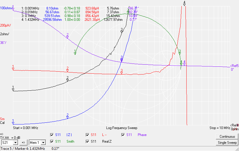
The first inductor is marked (color coded) 1000 µH. It has a DC resistance of 5.7 ohms measured using an ohm meter. Below is a plot of some curves for this component.

Curves for 1 mH inductor

The impedance (blue curve) goes up from low frequencies (as expected) and reaches 1000 ohms at about 200 kHz. It then stays above 1 kohm at least up to 10 MHz.

The inductance varies a little with frequency between 850 µH and 930 µH for frequencies between 1 kHz and 500 kHz.

The inductor is (parallel resonant) at around 1.4 MHz where it has a maximum impedance of nearly 30 kohms (a very uncertain value due to the S11 method’s inappropriateness of measuring impedances that are much larger or smaller than 50 ohms, the series S21-method should be used instead to get a more precise number).

The ESR (equivalent series resistance) is plotted in black. It goes up from 8.1 ohms at 1 kHz (remember it was 5.7 ohms at DC). This increase with frequency might be due both to skin effect and losses in the core.

This inductor has an impedance of above 500 ohms for frequencies between 100 kHz and at least 10 MHz, so if the communication is done in this frequency range, the loading through the inductor should be pretty low.

One caveat is that the inductance (and impedance) might go down when DC current is run through the inductor. This, as well as the simple IR drop across it is something to look out for in the application.

It might be possible to add a DC-blocks and a current source (that has to have high impedance over the frequency range of interest) to the test fixture to test the effect of a DC bias.

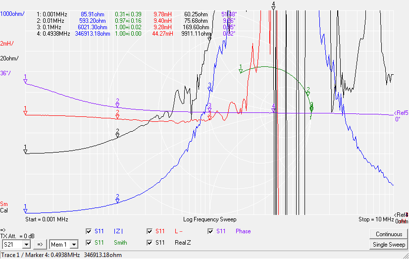
The second inductor is marked 10 mH and its curves are shown below. Note that some of the scales have been changed by a factor of 10. At DC, this inductor has a resistance of 60 ohms.

Curves for 10 mH inductor

This inductor might be suitable if very little current will be pulled through it (due to IR drop and saturation of the core), but it does of course provide higher impedance for lower frequencies. Above resonance, which happens around 500 kHz, the impedance comes back down again, so that it is 5 kohms around 3 MHz and 1.5 kohms at 10 MHz.

Vector Network Analyzer – a Christmas Present to Myself

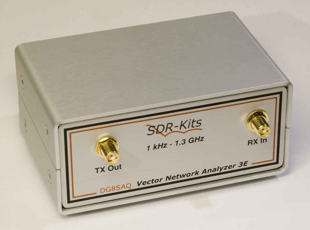
I bought myself a somewhat unusual Christmas present a few weeks ago, namely a vector network analyzer, VNA. All VNAs I had previously used were huge and very expensive instruments, but it turns out that there is an interesting alternative out there on the market. Tom Baier, a radio amateur with the call sign DG8SAQ has created a really neat product he calls the “VNWA 3E“. It is a VNA in a small box powered via USB and controlled by a PC.

VNWA 3E
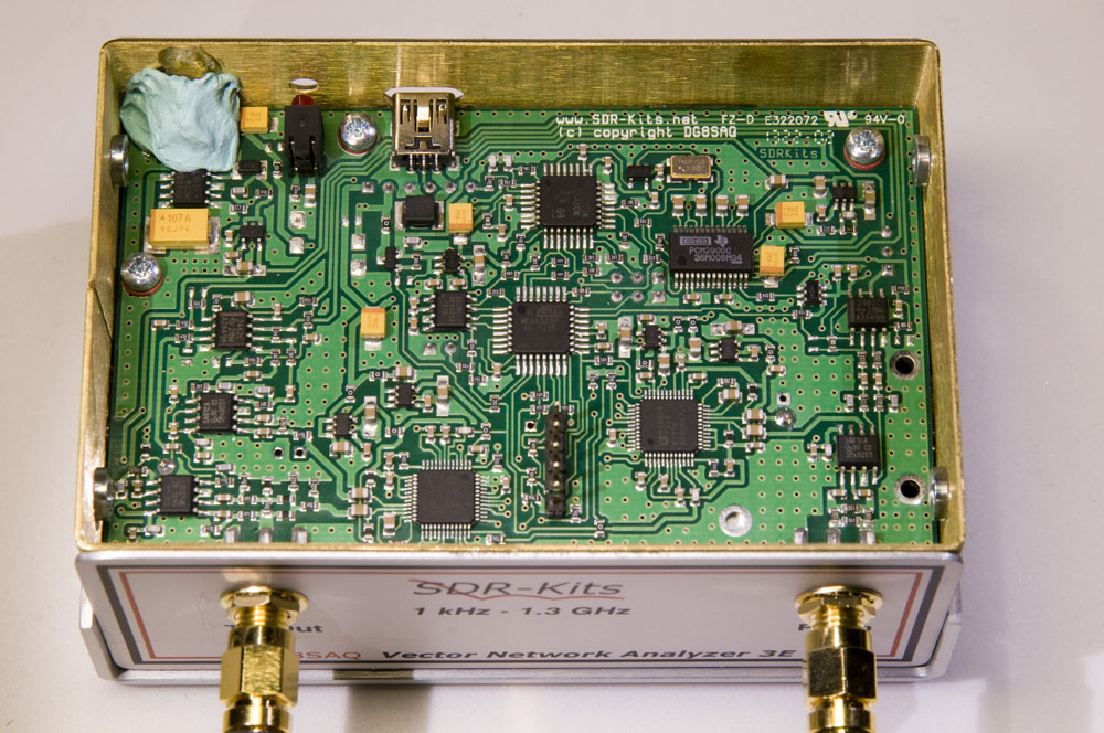
The network analyzer VNWA 3E

(I do not know why everybody insist on using the abbreviation VNWA instead of VNA for this particular VNA, but it seems like VNWA has become the accepted name for this device, so I will use it when referring to this product and not VNAs in general.)

Technical description

The VNWA design itself is very clever as it covers a relatively large frequency range while still being orders of magnitude cheaper than traditional VNAs. It achieves this through a minimalistic design and a combination of using harmonic overtones of the frequency synthesizers, overclocking the synthesizers outside of their specified frequency range and also using mixers outside of their specified operating range. The main downside of this approach seems to be that the dynamic range suffers for frequencies above 500 MHz. Also, the maximum output power is really low at -17 dBm at 1 MHz and less for higher frequencies. This however is usually not a major problem.

AD9859 10-bit DDS (direct digital synthesis) chips are used for both the RF and the LO oscillators. These are specified for clock frequencies of up to 400 MHz, so normally they could only be used to generate signals up to a bit below 200 MHz. But it turns out they always seem to work fine when overclocked up to 720 MHz, and by utilizing harmonics, much higher frequencies can be probed than one would originally expect.

An IF of between 1 kHz and 12 kHz is used and it is sampled by an audio ADC. There does not seem to be any explicit IF filter in the design and one can in particular not select between different IF bandwidths as is possible on most other VNAs. It is however possible to select the measurement time at each frequency point.

The VNWA 3E can measure both S11 and S21 (reflected and through) S-parameters at the same time since it contains an expansion board with an extra audio ADC. To measure S22 and S12 (reflection from output and reverse transmission) the connections to the device under test (DUT) have to be manually swapped.

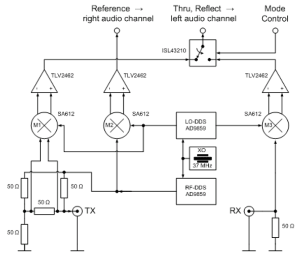
Below is a partial block diagram of an earlier version of the VNWA where a PC soundcard was used as the sampler of the IF and reference signals.

VNWA block diagram
Old VNWA block diagram

Due to the shortcuts taken in the design of the VNWA, there are thus some shortcomings and a few features missing that one would find in a traditional VNA, but there are also many useful features provided in the software that I have not seen in other VNAs. Considering the price, I think the instrument is a bargain if you want to make measurements in the 200 Hz to 1.3 GHz range and can live with a dynamic range of about 50 dB above 500 MHz.

Whistling inductor

When I received the VNWA, I was first struck by its small size. I had expected it to be small, but not so small. It is only 10.4 cm wide. The installation went fine, but there was an audible whistling noise coming from the device. It sounded like noise I had previously heard from some DC/DC-converters. I contacted SDR-kits where I bought the VNWA and was told that the noise problem could be solved by putting a drop of glue on top of the inductor of a DC/DC converter.

I took the unit apart (which is very simple to do) and put some hot melt glue on the suspect inductor, glueing it to the side wall. On top of that I put some Tack-It. This largely eliminated the noise, although I can still hear it if I listen close to the device. Looking at the circuitry around the inductor, it is apparent that a MAX632 is used as a step-up converter and this chip seems both expensive and outdated. It switches at 45 kHz and the regulation is done by skipping cycles, rather than by adjusting the duty cycle. This probably leads to the ripple current having lots of frequency content in the audible spectrum, which the inductor converts to sound. A more modern step-up-regulator would probably both reduce the cost and get rid of the noise. Below is a photo showing the inductor covered in glue and Tack-It.

Glued inductor
The opened VNWA with the glued inductor at the top left.

Some tests

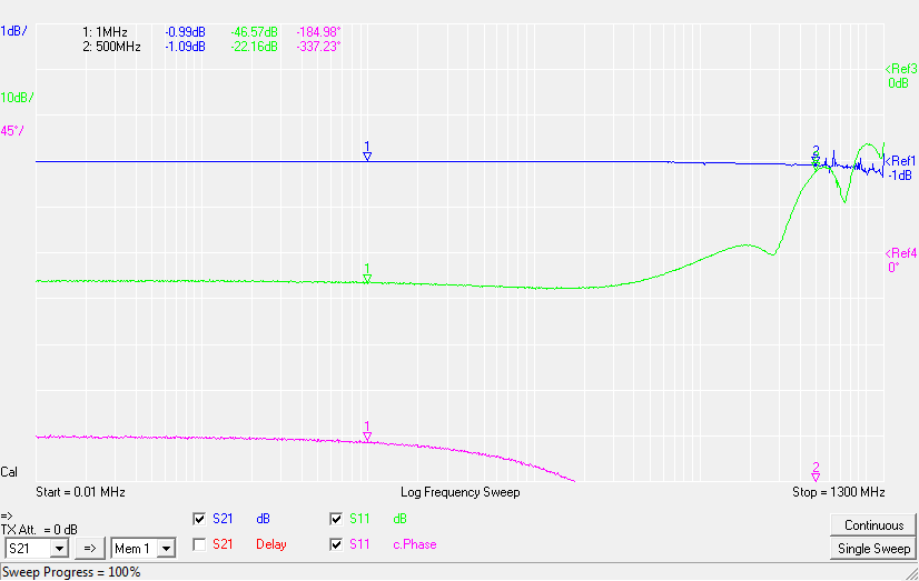
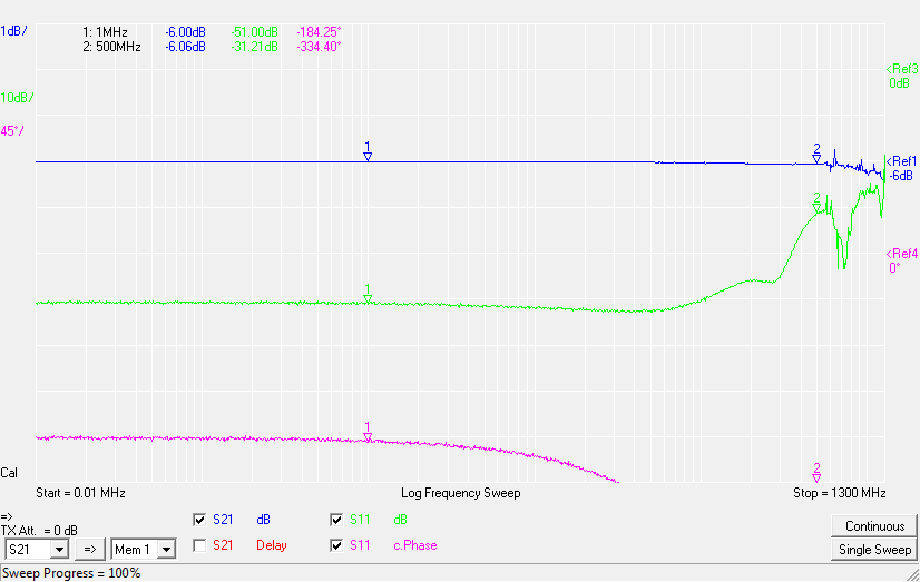
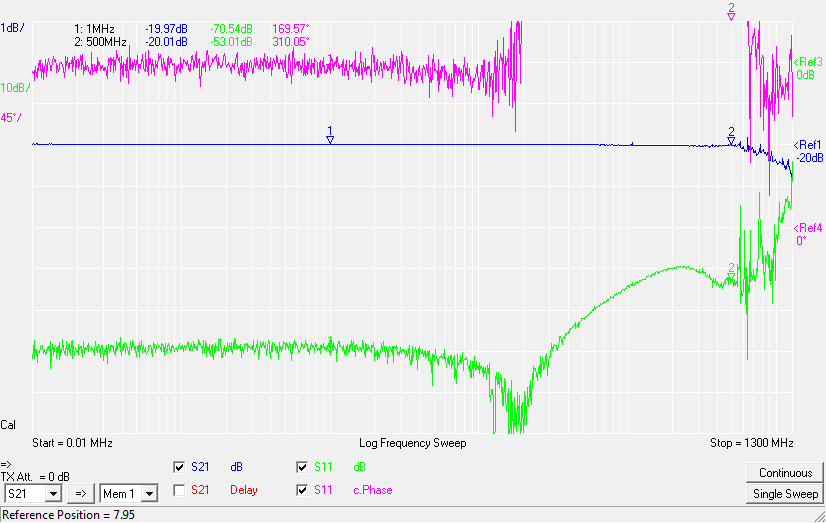
To try out my new toy, I did a couple of measurements.  First I tested three different attenuators.

1 dB att
Plot of 1 dB attenuator (VAT-1W2 from Minicircuits)
6 dB attenuator plot
Plot of 6 dB attenuator (VAT-6W2 from Minicircuits)
20 dB attenuator plot
Plot of 20 dB attenuator (VAT-20+ from Minicircuits)

All of these three attenuators are specified to have about 0.2 dB excess loss at 1 GHz. This is approximately what the VNWA shows for the 1 and 6 dB attenuators, but it looks more like 0.4 dB extra loss for the 20 dB attenuator. Also, the S21 (transmission) curve looks a little jagged above 500 MHz, which is probably the decreased sensitivity and accuracy in this frequency range showing up.

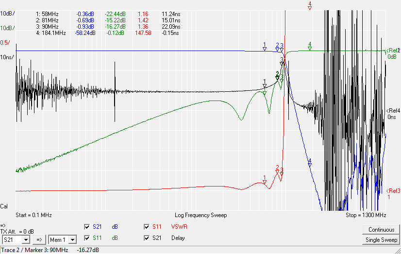
Next I tried a 90 MHz low-pass filter. Comparing this to the datasheet, it seems like the filter has less loss at 90 MHz than what is typical. The 3 dB frequency is actually 95.8 MHz.  VSWR in the pass band is also better than typical (< 1.42 whereas the DS says < 1.7). The stopband attenuation should be greater than 70 dB between 230 and 400 MHz, and this is also shown by the VNWA. The datasheet gives no data above 400 MHz and I do not trust the VNWA to say much about attenuations larger than 50 dB above 500 MHz.

90 MHz low-pass filter
Plot of 90 MHz low-pass filter (SLP-90 from Minicircuits)

Component measurements

One of the great things with a VNA is that it can be used to measure component parameters over a range of frequencies. It can therefore be used to measure e.g. inductance and capacitance. The VNWA actually has a built-in LCR-meter function measuring at a single (but selectable) frequency, but I prefer to do a sweep and see how the measured value changes with frequency. In that way it becomes obvious if the component that is tested behaves in the expected manner (like a capacitor keeping its capacitance over a range of frequencies).

There are different ways to use a VNA to measure impedance. Basically, one can base the measurements on reflected waves (S11) or transmitted waves (S21). The S11 method has the advantage that only one cable is needed, while the S21 method requires two cables, but has advantages in terms of easier calibration and more precise results when the impedance is very high or very low compared to the system impedance of 50 ohms. When doing S21 impedance measurements, the unknown impedance can either be placed in series with the signal path (good for high impedances) or shunting the signal to ground (good for low impedances).

The VNWA software has built-in support to convert S11-data to capacitance and inductance but does not seem to have direct support for the S21 methods of component measurements. A great feature though is that it is possible to define custom formulas that do the conversion from S-parameters to e.g. capacitance or inductance, so the results of S21-based component measurements can be easily plotted.

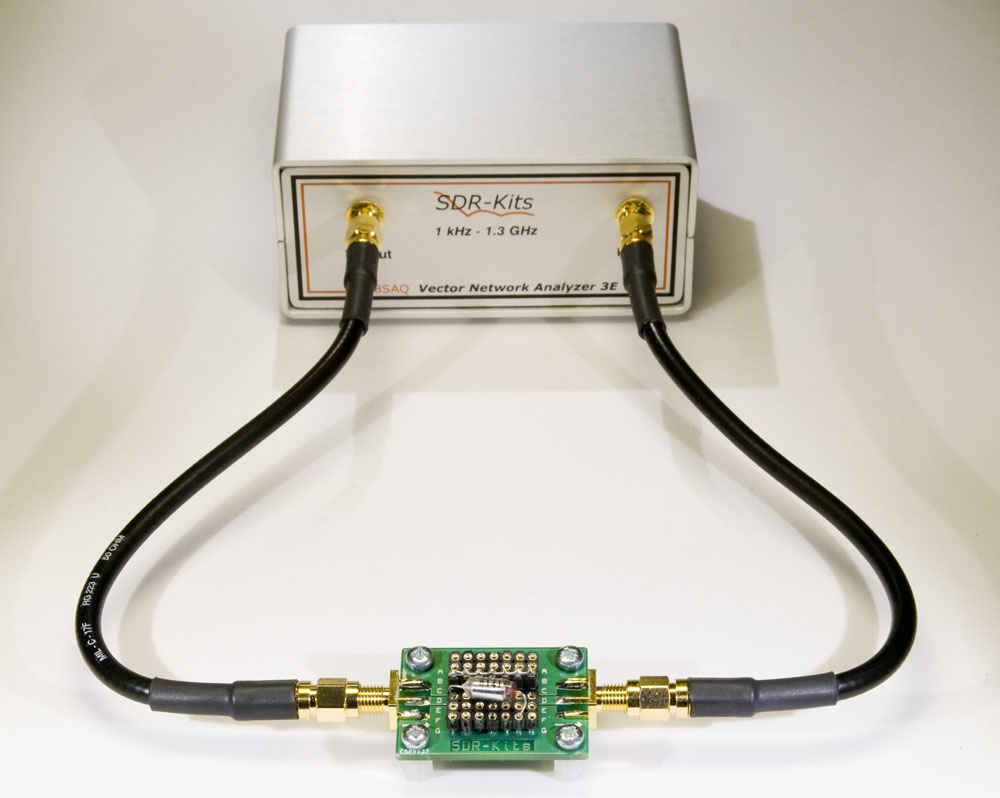
I tested a few different components using an educational test fixture I bought together with the VNA and seemed to get good results. Below is a picture of the VNWA with the test fixture in front.

VNWA with test fixture
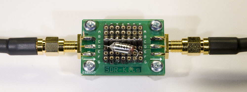
Closeup of the test fixture

Clearly, the fixture is not designed to have low parasitics at high frequencies, but it should be useful up to at least a few MHz.

First I tested two inductors, one that I found in a DC/DC converter I discussed in a previous blog post and a random toroid I had in the junk bin.

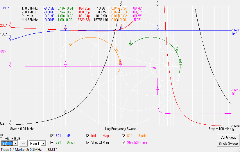
I connected the inductor from the signal to ground, shunting the transmitted signal. Six different curves are plotted simultaneously:

  • S21 is plotted both as magnitude and in a Smith chart,
  • the inductance calculated from the S21-parameter,
  • the magnitude of the shunting impedance (unfortunately it is not possible to use a logarithmic Y-axis when plotting, unless you plot dB),
  • S11 in a Smith chart and
  • the phase of the shunting impedance.

The reference levels and values can be seen at the right side of the plot while the per-division values can be seen on the left.

The calculated inductance drops slowly over the frequency range from 10 kHz (165 µH) via 100 kHz (160 µH) to 400 kHz before it approaches resonance at 4.7 MHz. The phase of the shunting impedance is close to 90 degrees up to 2-3 MHz. The inductance seems to be around 160 µH based on this test.

Plot of inductor from DC/DC converter

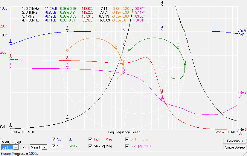
The toroid gave the below plot. The inductance is dropping from 10 kHz (114 µH) to 1 MHz (108 µH) where the phase is 70 degrees, indicating quite a bit of loss. This inductor has much more loss at higher frequencies than the previous one and is perhaps intended as a choke rather than as a low-loss inductor for e.g. a DC/DC converter.

Plot of random toroid inductor
Plot of a random toroid inductor

I also had a few low-tolerance capacitors and it seemed like a good idea to check what readings the VNWA would give when presented with these.

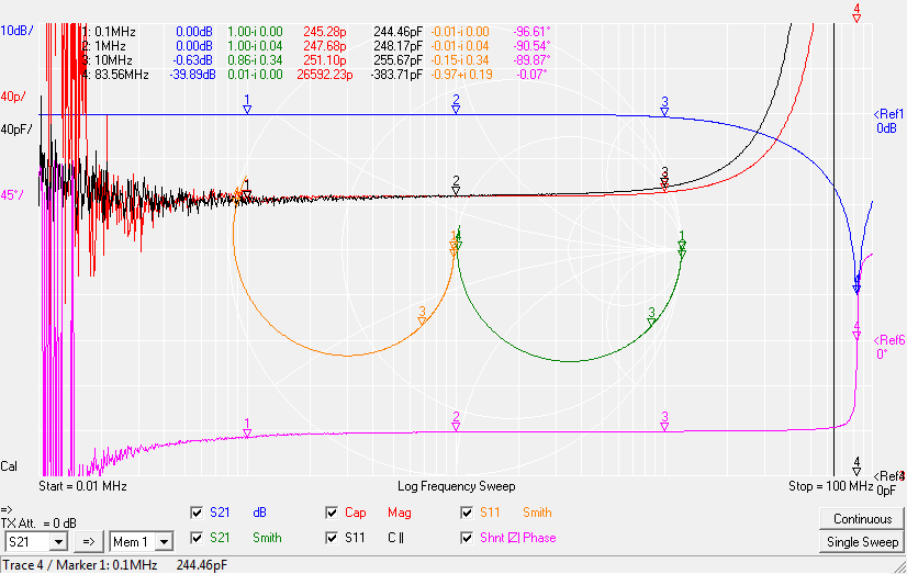
The first one is marked 246 pF 0.5%, so it should have a capacitance between 244.8 and 247.2 pF. I have plotted not only the capacitance calculated using my S21-based formula, but also the built-in S11-based formula. Both formulas give realistic values at the flat portion of the graphs with 247.7 pF for S21 and 248.2 pF for S11 at 1 MHz. A little smoothing would have been appropriate to get better readings at lower frequencies, although neither measurement method is suitable for measuring 246 pF below 100 kHz. Putting the capacitor in series would have given better LF-results for the S21 approach.

Capacitor plot
Plot of 246 pF +/- 0.5% capacitor

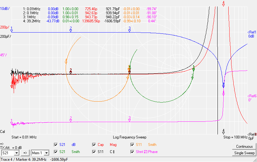
The second capacitor is marked 942 pF +/- 0.3% (thus 939.2 to 944.8 pF). A handheld component tester measured this as 944 pF. The S21 approach gives values within the tolerance range for both 100 kHz and 1 MHz, whereas the S11 approach is a little more variable.

Capacitor plot
Plot of 942 pF +/- 0.3% capacitor

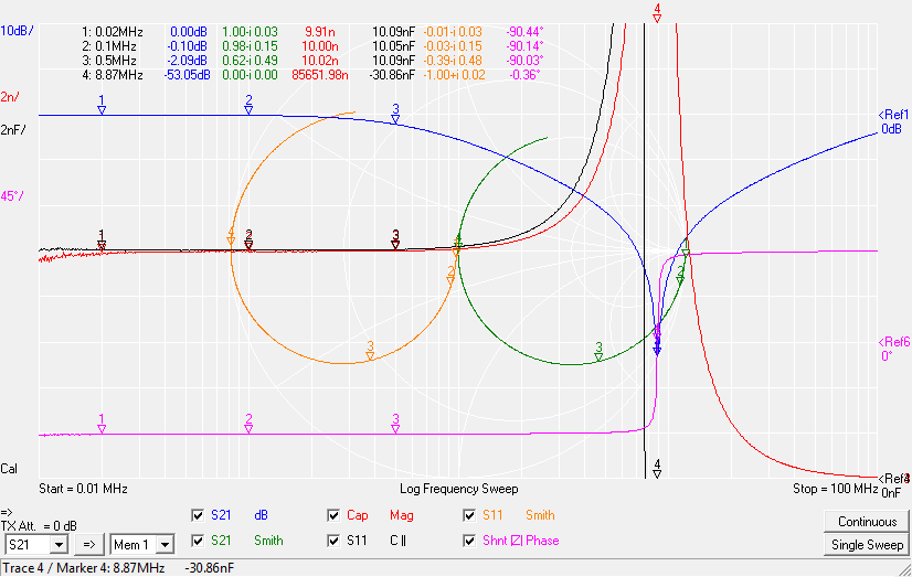
The next capacitor is marked 10 nF +/- 0.5% (thus 9.95 to 10.05 nF). S21 gives values within this range for both 100 kHz and 500 kHz.

Capacitor plot
Plot of 10 nF +/- 0.5% capacitor

So in all, it seems like the VNWA is pretty useful to measure capacitances and inductances like these. The tolerance is probably better than 1% if the calibration and the measurements are made carefully.

A great Christmas present!