I wanted to build a capacitive detector that can sense the proximity of a conductive object, like a finger or a piece of metal. I have some idea what I could use such a detector for, but the following prototyping exercise quickly diverged into a quick just-for-fun hack.
There are many ways to build capacitive detectors. A very common one is the variety of touch sensing solutions provided for micro controllers from companies like Atmel (QTouch), NXP, Cypress (CapSense), Microchip (mTouch) and others. In addition to these proprietary solutions, there are also some open source micro controller based solutions, some using ADC inputs and others using just plain digital I/O pins.
Another solution would be to build an oscillator whose frequency is dependent on the (small) capacitance that one is trying to sense. This seemed appealing to me as i felt like building some analog RF circuitry, so I decided to go down this route. Since the capacitance that is to be sensed is pretty small, on the order of a few pF, a relatively high oscillation frequency is required to have the change in capacitance correspond to a reasonably large change in oscillation frequency.
Again, there are many options on how to build an oscillator. I decided to use an incarnation of a Colpitts oscillator, namely the common collector type. The general schematics is shown below.
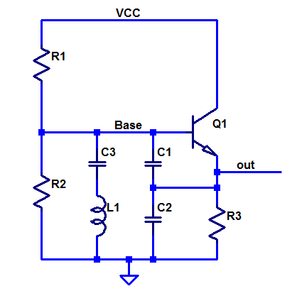
R1 and R2 (and R3) provide bias to the transistor. C1 and C2 provide feedback while L1 together with the series combination of C1 and C2 determine the oscillation frequency. C3 has a value large enough to act like a short at the oscillation frequency and prevents the inductor from ruining the biasing of the transistor.
After some quick simulations in LTspice, I ended up with the below circuit.
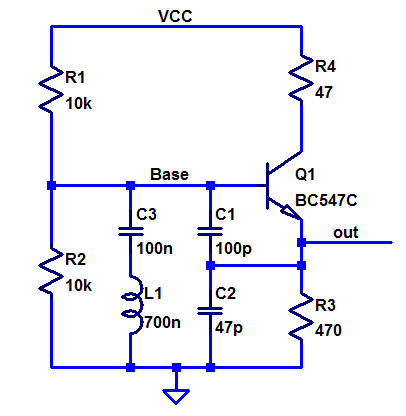
The addition of R4 helps to make the output more sinusoidal as it provides negative feedback at high frequencies via the miller capacitance between the collector and base of Q1. The oscillation frequency with the above component values is around 34 MHz.
So which node do we use as the sensing node? One could consider using either the output or the node labeled Base, but it is probably better to use the Base as adding capacitance there does not change the feedback ratio, while adding capacitance at the output would change the feedback and possibly risk stopping the oscillation. To use the Base as a sensor, it needs to be connected to a relatively large metal plate whose capacitance will then be modulated by nearby conductive objects.
Adding a pF at the Base will change the frequency by about 500 kHz. This is certainly easy to detect if one is using e.g. a counter input of a fast micro controller.
I decided however to make the change even easier to detect (especially by slower micro controllers) by mixing the output of the variable oscillator with the output of a fixed oscillator with a slightly lower frequency to produce a signal with a frequency that is the difference between the two frequencies. The difference signal will thus see a much larger relative shift in frequency than the initial signal.
Building another identical oscillator (but without the capacitive sensing plate) is straightforward. This oscillator should however be trimmable so that it can be adjusted to have a frequency suitably below the frequency of the sensing oscillator. Typically one would do this with a trimming capacitor, but as I was building the circuits using parts from my junk bin and I had inductors with trimmable cores, I used one of those instead.
The main question that remains is how to build the mixer that shall essentially multiply the signals from the two oscillators to produce tones at the sum and difference frequencies of the original signals. There are of course many mixer circuits on the market and one can also build them using discrete components. I decided however to do it in a somewhat non-conventional manner, namely by using an XOR gate. The signals from the oscillators happen to have enough amplitude so that they can drive TTL (or CMOS) gates and I had a bunch of old 74LS86 quad XOR gates in 14-pin DIL packages. Ideally one would like to have gates with schmitt trigger inputs when driving them with analog signals. 74HC86 are XOR gates with such inputs, but since I did not have any of those laying around and did not feel like ordering any just for this quick hack, I went with the somewhat inferior (for this purpose) 74LS86.
What remains is to low-pass filter the output of the XOR gate to get rid of the high-frequency mixing products. I used a simple RC-filter for this, although an RLC-filter would have been more elegant and effective. To tidy up the signal and get a nice buffered square wave I used another of the XOR gates in the same package. Again it would have been nice to have a gate with a schmitt trigger input.
The complete circuit diagram is shown below.
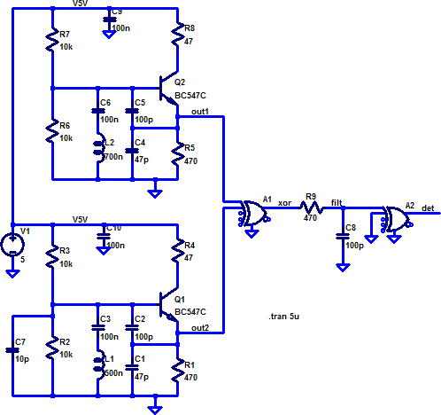
C7 is meant to represent the sensor plate. The decoupling capacitors C9 and C10 have no effect in the simulation but are good to have in reality as there is plenty of inductance in the wires from the power supply to the circuit.
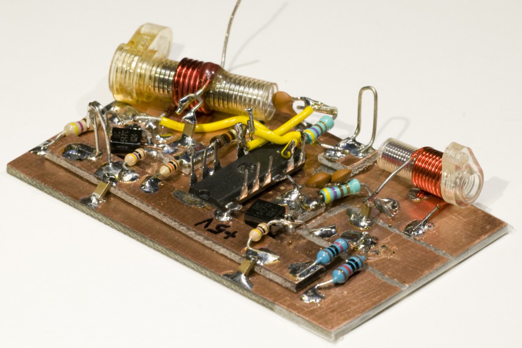
I built the whole thing on single-sided copper clad board as shown below.
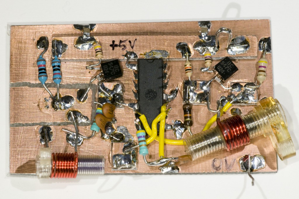
Here is a labeled picture of the board:
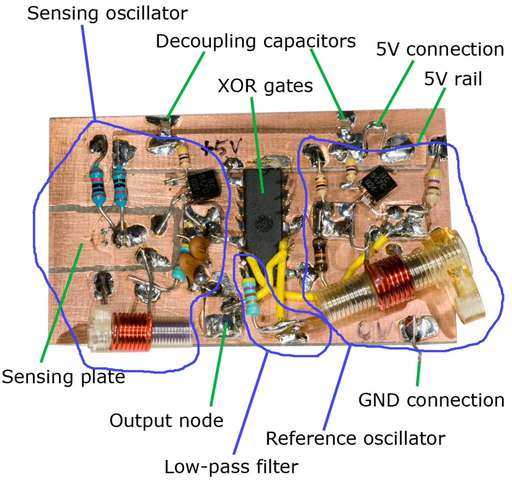
For the 5 V rail I used another slice of copper clad board on top (using hot glue) of the main board. Similarly, I glued small pieces of copper clad to serve as the base and emitter nodes of the transistors. For the sensing node, I milled out a slice of the main ground plane using a hand-held Dremel. The 74LS86 XOR gate package is placed upside down to provide easy access to the pins. The GND pin is bent down and soldered to the GND plane while the VCC pin is bent and soldered to the 5V rail. A drawing of the pinout when viewed from below is very useful when wiring up the XOR gates like this. I left unused XOR inputs floating, which is not exactly good practice, but generally works fine for 74LS chips. I would not have done that with a CMOS chip like 74HC86.
I used components I had on hand throughout, so there is a mix of old and new components. The inductors probably come from some radio or TV set that I disassembled 25 or more years ago. Some of the capacitors are surface mount and perhaps hard to see. The base-emitter capacitors are 0603 types soldered directly on the legs of the transistors.
So does it work?
Yes, it does. In fact I was surprised how little trouble I had getting the oscillators to oscillate and getting everything connected right. I started out by building the sense oscillator and it worked right away. When I later added the reference oscillator and the XOR gates they also worked without any issues. No troubleshooting opportunities this time.
Below are oscilloscope screenshots showing the signals at the output of the mixing XOR gate (CH1, yellow), at the output of the low-pass filter (CH2 blue) and at the output of the buffering XOR gate (CH3, green). The first plot shows the circuit free-running without any object close to the sensing plate and the second plot shows how the frequency is reduced when a metal object is close to the sensing plate.
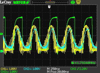
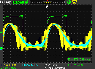
In the first case the mixed signal has a frequency of 1.79 MHz while it has been reduced to 671 kHz in the second case. The XOR gate is working at frequencies close to the limit of its abilities (and with input signals with poor slew rate at that), so it does not reach full swing (yellow trace), but it is still good enough for this purpose.
Cool circuit! I was just curious. Why is it common practice to construct prototypes of RF circuits using this type of point to point and landing pad method? Why not use a through-hole stripboard as is common for digital prototypes? Is it for better grounding?
Hi Danjel,
There are several reasons to use this build technique which is usually called “Manhattan style”.
When the frequency goes up, inductance becomes more of a concern, since the impedance of any given inductance is proportional to frequency. This means that you will not have essentially 0 ohms impedance between the ends of a piece of wire as you will at DC and low frequencies. Adding random unwanted impedances in the ground leads of components can easily degrade the performance of many circuits or even prevent them from working at all, so at high frequencies it is nice to have a construction method that more or less eliminates the inductance. The wide ground plane has a very low inductance compared to wires and the strips of stripboards.
Also, ground is almost always the node that has the largest number of connections to it, so it is convenient to have ground available everywhere.
Another advantage is that all connections are visible and made from the top of the design, so it is relatively easy to see how everything is connected. You also do not have to constantly flip the board over when building it.
This is certainly not the only way of building working RF prototypes, but I find that it is reliable, straightforward and convenient.
Here are two links to documentation made by K7QO about how to go about building stuff using the Manhattan style:
http://www.qrpme.com/docs/K7QO%20Manhattan.pdf
http://www.k7qo.net/chapter-24.pdf
I agree 100%. Manhattan style is supr clear and transparent way of prototyping. Besides of all those inductance and parasitic capacitances problems i hate protoboards. You end up with net of wires and every mistake costs you a time. Qrpme has a nice solder islands ready made for use. 73! SP5SMH
This is the first time I hear about “Manhattan Style” prototyping, as I am not a native english speaker. It looks so artistic, I like it, congratulations!
And thank you for your detailed explanation of the circuit and the components used, it’s very useful.