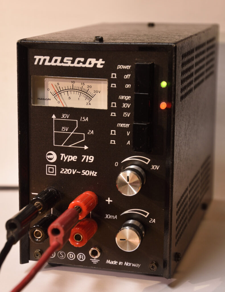
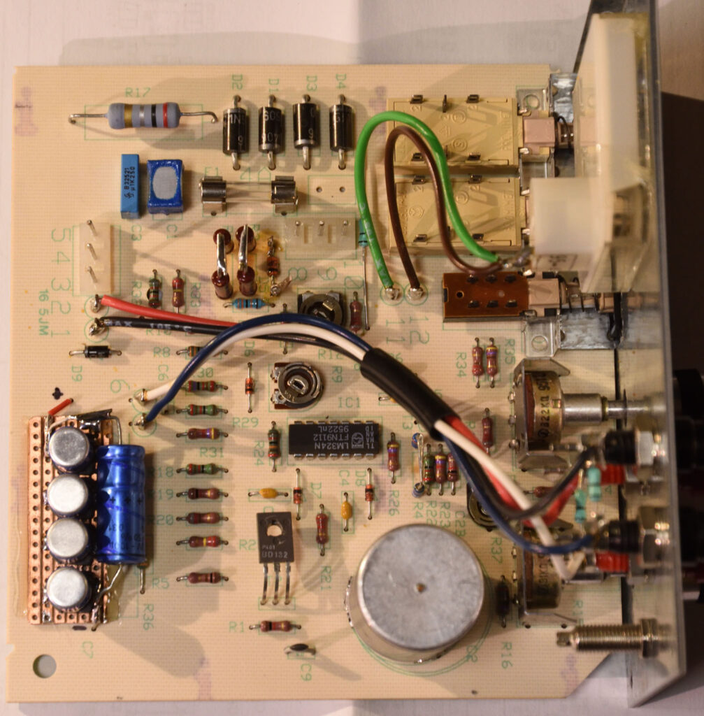
Mascot 719 is an old (probably designed in the 1980s or early 90s) and simple lab power supply. It can output 0-15 V at up to 2 A and 0-30 V at up to 1.5 A. I received a broken unit from a friend and set out to fix it.
At first glance, it was obvious that the resistor R4 had burned up. It was discolored, so it was unclear what its color code was, but it looked like 100 ohms, so I put a new 100 ohm, ¼ W resistor in its place. I also noticed that the solder joints of the front panel pots for setting voltage and current limits were very poorly soldered, so I fixed that as well.
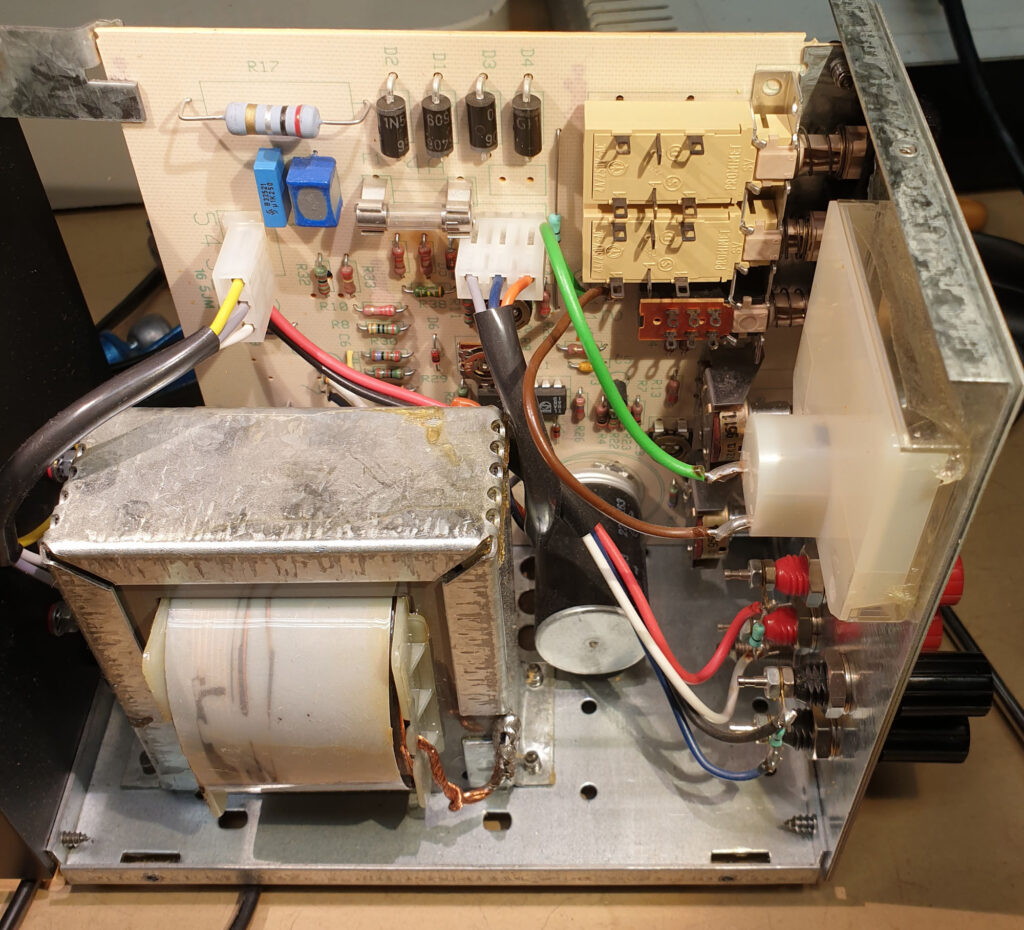
The area around R2, R3 and D5 was discolored from heat, but the components seemed to have reasonable values when checked with a multimeter, so I let them be. The output transistor on the heatsink in the back checked out OK with simple diode tests and so did T2, a BD136 driving it, as well as T3, a BC547B driving T2.
After powering it on again, the new R4 quickly let out its smoke and simultaneously desoldered itself from the board. At the same time T3 and T2 died.
Schematics
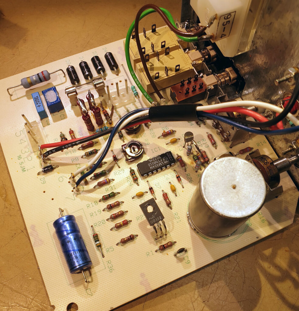
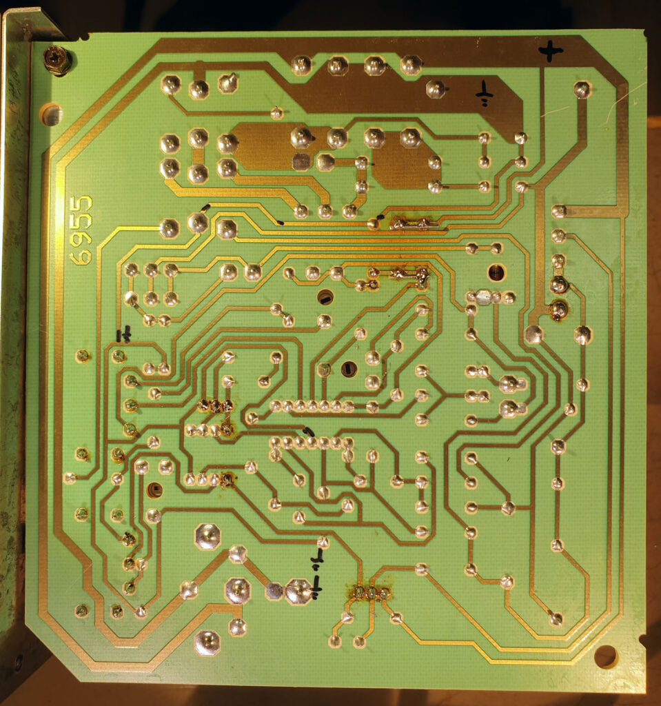
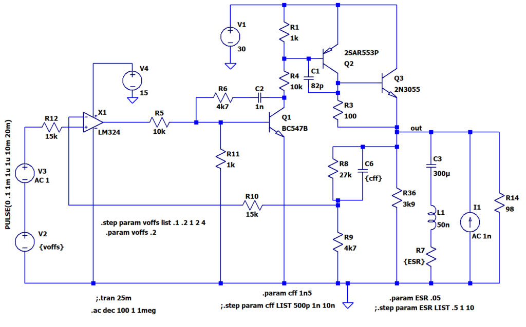
At this point I decided it was time to trace out the schematics so that I could figure out how the supply was supposed to work. This seemed doable, since the board is a rather simple 1-layer board with about 40 large through-hole components. Still, the process took several hours split over three days. Repeatedly rearranging the schematics and finding and correcting mistakes were major parts of the work.
Here is the result (click for a higher resolution image):
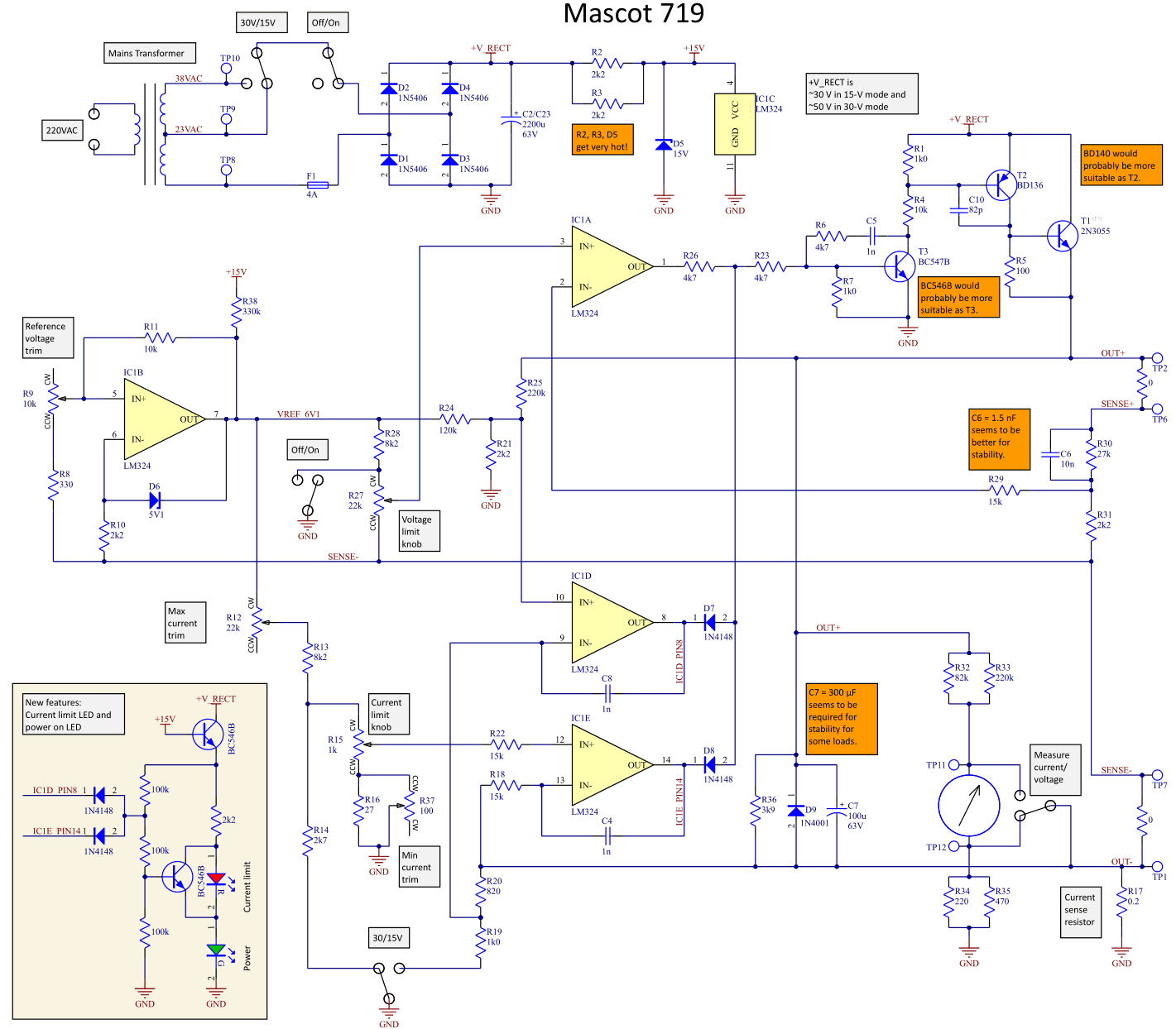
The “brains” of the unit is a quad opamp, LM324. One section of it, IC1A, controls the output voltage based on the setting of the front panel pot R27. LM324 is of course not powerful enough to directly drive the output, so it does this via a cascade of three transistors, T3 (BC547B), T2 (BD136) and T1 (2N3055).
When the output of IC1A increases, the base current of T3 increases and so does the collector current through R4 and therefore also the base current of T2. R4 affects the voltage gain from base to collector of T3 and since there is negative AC feedback via C5 and R6, it affects the loop dynamics. It also limits the maximum amount of current that T3 can sink.
+V_RECT is around 30 V in the 15-V mode and around 50 V in the 30-V mode. If the control loop decides it needs to raise the output by a lot and therefore applies a lot of base current to T3, the current through R4 can get very large if R4 is only 100 ohms, and it is easy to see that the power dissipation can get very far outside of the rated ¼ W. In the worst case, almost the full +V_RECT is applied across R4, which means more than 20 W in the 30-V mode and almost 10 W in the 15-V mode. I think something along these lines is what happened, but I do not know for sure why it happened. One hypothesis is that T2 was broken so that it did not provide any collector current and therefore T1 did not turn, keeping the output low while the control loop tried harder and harder to increase the output by increasing the base current to T3 and therefore pulling larger and larger currents through the poor R4.
To prevent this from happening, I decided to increase R4. The supply shall be able to provide 2 A and T1 has a minimum current gain of 20 according to a datasheet, so T1’s base current needs to be able to reach at least 100 mA. T2 has a minimum current gain of 40, which means its base current needs to be up to 2.5 mA. With 20 V across R4 (some margin from 30 V) it could be up to 8 kohms. 50 V across 8 kohms (should never happen, but better safe than sorry) dissipates 0.31 W, so a single ¼ W resistor is perhaps not enough. I decided to put two 3.9 kohm resistors in series as R4. Another option would have been to select 10 k which would dissipate precisely 0.25 W at 50 V. I have written 10 k in the schematic.
It is possible that 10 k is actually the original value for R4. The color ring that indicates the number of zeros on the original resistor is discolored due to the overheating, so it is hard to tell whether it was brown (as I initially assumed) or perhaps orange. The difference is 100 ohms vs 10 kohms…
I put in a new BC547B as T3, put 2*3k9 as R4 and replaced T2 with a BD132 as I did not have any BD136 on hand. BD132 seems to be have very similar specifications.
After this the unit basically worked and no smoke was emitted!
Adjustments
However, it was possible to turn up the output to more than 30 V and the current limit did max out at more than 2 A in the 15-V mode. Maybe this is good and useful, but I wanted to follow the original specs for the supply, so I turned to the schematics to figure out how to adjust the trimmer pots to align the unit.
IC1B forms an adjustable voltage reference that creates a voltage referred to SENSE-. This reference voltage (which I called VREF_6V1 in the schematics) determines the maximum output voltage setting since the potentiometer that sets the output voltage, R27, is connected across it (via R28). The output voltage is scaled down by R30/R31 by a factor of 0.15, so when the output is 30 V, the negative input to IC1A becomes 4.45 V. The upper end of R27 is at 0.73 times the reference voltage and to make it 4.45 V, the reference voltage must be 6.1 V.
So, the first step is to trim R9 until the reference voltage (pin 7 of IC1B) is at 6.1 V. Alternatively, and perhaps better (to account for tolerances in the pot and resistors): Put the supply in the 30-V mode, crank up the voltage setting knob to max and adjust R9 until the output voltage is 30 V.
To trim the maximum output current, R12 has to be adjusted. One way of doing this is to set the supply in the 15-V mode, crank up the voltage and current knobs to max and connect a power resistor of between 5 and 7.5 ohms to the output. An ammeter should be used to measure the current through the load while R12 is adjusted to limit the current to 2 A.
There is also a minimum current limit according to the front panel, namely 30 mA. This is trimmed by adjusting R37 in the following manner:
Set the current limit to minimum. Turn down the voltage to something suitably low, like 3 V. Connect the ammeter directly across the output (or in series with a limiting resistor) and adjust R37 until the ammeter reads 30 mA.
Other tweaks
Since the series resistors in the crude shunt zener voltage reference R2/R3/D5 gets very hot, particularly in the 30-V mode, I decided to replace them with several resistors to better handle the power dissipation. With +V_RECT at 50 V, 35 V lies across R2 and R3 which are both 2.2 kohms, so the power dissipation is more than 0.5 W. Not good for resistors that seem to have the ordinary ¼ W rating. My solution was to replace each of R2 and R3 with a string of two 1.2 kohm resistors with a rating of at least 0.5 W each, which I had on hand. The slightly higher resulting resistance is hardly of any importance. I also soldered ~10 mm stumps of used copper desoldering braid to the legs of D5 to help it get rid of heat more easily.
In general, it is a good idea to replace electrolytic capacitors in old equipment, since electrolytics tend to degrade over time. I measured the ripple on +V_RECT and found the valleys at maximum load to always be at least 7 V above the maximum rated output voltage (15 or 30 V depending on setting), so it does not seem to be necessary to replace C2 to smooth +V_RECT further. I did some changes to C7 however. See the section on stability below.
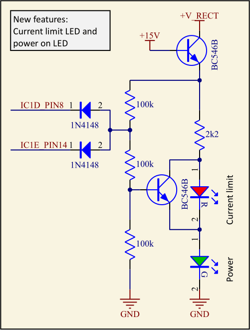
An extra feature one could quite easily add is an LED that lights up when the current limit kicks in. To do this, one needs to understand how the current limiting works:
Current limiting
IC1E handles the normal adjustable current limit. When the current is lower than the set value, its output is high (14 V or so) and it does not affect the output voltage since D7 therefore is back-biased and does not conduct. As soon as the voltage across the current-measuring resistor R17 reaches the level set by the current limit potentiometer R15, the output of IC1E goes low(er) and diverts current from the base of T3 to limit the output voltage and thereby the output current. A switch cleverly connects R14 across the potentiometer R15 when in the 30-V mode. This reduces the voltage at the top of R15 so that the maximum current one can set using R15 is reduced from 2 A to 1.5 A.
IC1D acts as another current limiter that works in a similar way. Its purpose however is to reduce the maximum allowed output current if the output voltage is low. (Curves printed on the front panel illustrate this behavior.) As in any linear regulator, the output transistor (T1) is subjected to the highest power dissipation when the output current is high while at the same time the output voltage is low. To limit the dissipation in T1, it therefore makes sense to not allow as high output current when the output voltage is low. The resistors R21, R24 and R25 form a voltage divider that scales the output voltage so that it can be used by IC1D to compare with the voltage drop across the current sensor R17. In the 15-V mode, a switch engages the voltage divider R20/R19 to scale down the voltage drop across R17 so that higher currents are allowed before the protection kicks in.
Both IC1D and IC1E are connected via diodes to a node near the base of T3 and can therefore override the voltage regulating IC1A and reduce the output voltage (and thereby current) by reducing the base current to T3. The diodes prevent these opamps from ever increasing the output voltage above what IC1A wants it to be, they can just reduce it when necessary.
Now that we understand the current regulating parts, we can see that when current limiting kicks in, either of IC1D or IC1E pulls their outputs low. To signal that this is happening, we can build an OR-gate that controls an LED by connecting the cathodes of two diodes to each of these outputs (pins 8 and 14), join the anodes and connect them to the LED in series with a resistor connected to +15V. This works, but I also wanted an LED that lights up when the power is on and, furthermore, I found it wasteful to have so much voltage headroom (up to 50 V originally) and use separate currents from this voltage to power two different LEDs. I therefore came up with a somewhat more complex solution shown below. The two LEDs are connected in series, so that they use the same current. A transistor controlled by the diode OR-gate shorts out the current limit LED when no current limiting is going on. This changes the brightness of the power LED very slightly, but this is almost imperceptible.
Stability
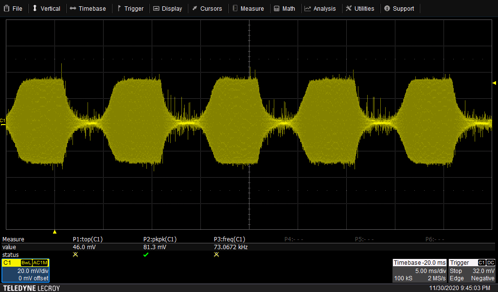
Feedback systems like voltage and current regulators can be unstable, so I wanted to check whether this power supply suffered from that. I varied the output voltage from 0 V to max while loading the output with either nothing, 22 ohms or 7 ohms. I also varied the current limit setting.
Unfortunately, there were tendencies of instability for low output voltages (0.5 V to 4 V) with a load of 7 ohms. A roughly 70 kHz tone of up to 150 mVpp appeared at the output. Not good.
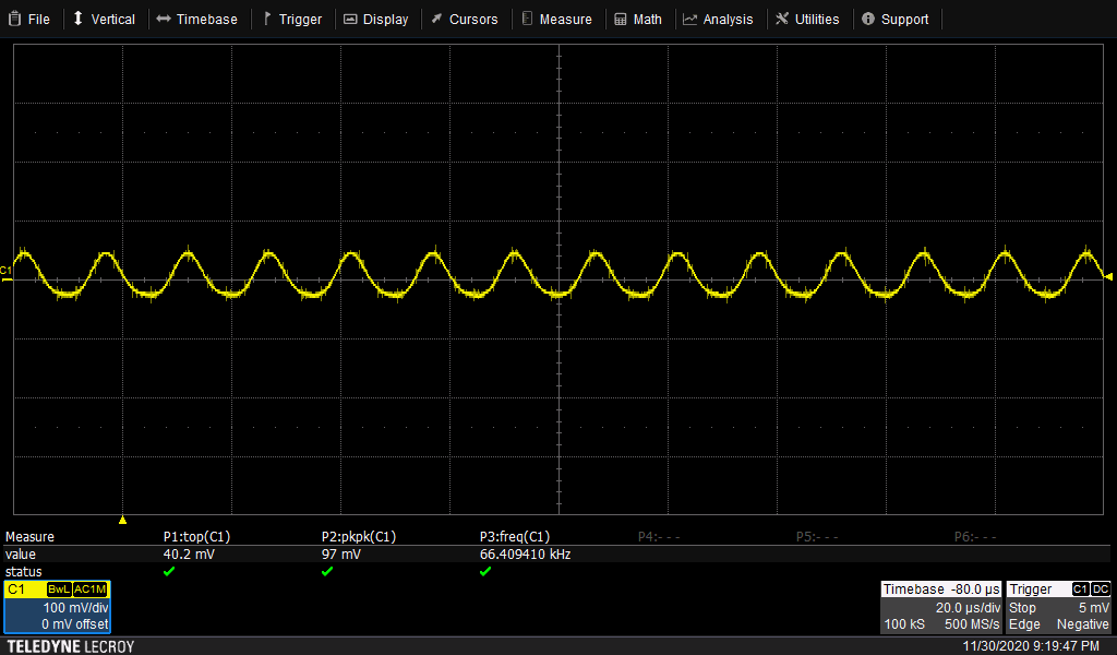
I modeled the voltage control loop in LTSpice and were able to see a similar behavior there as well.
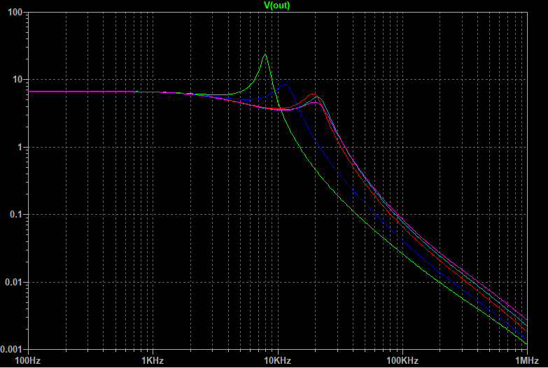
After lots of back-and-forth between LTSpice and the real board, I came up with a solution that did not seem to oscillate under any of my test conditions. In addition to the original 100 µF capacitor across the output, I added four more 47 µF, 63 V capacitors. I also had to change C6 from 10 nF to 1.5 nF. I still do not fully trust the supply to always be perfectly stable, but it is certainly much better than before this modification.
Some observations
+V_RECT is about 50 V in the 30-V mode. BD136 (T2) is rated to V_CEO and V_CBO = 45 V. This is marginal to say the least, as almost the entire +V_RECT will be across the transistor when the output is at 0 V. BD140 which has a rating of 80 V seems like a much better choice as T2 and an upgrade seems like a very good idea. Maybe this is what caused the original T2 to fail?
BC547B (T3) also has a V_CEO rating of 45 V, so this too is not a good choice in a position where it can be subjected to 50 V. I think BC546B with its higher voltage rating would be much safer.
The power supply was designed while the mains voltage was 220 V (it says 220V~ 50Hz on the front). It has since been raised to 230 V (in Sweden this happened in 1988, maybe it was the same in Norway?), which results in a slightly higher +V_RECT, but even with 220 V, the voltage would have been too high for a BD136 and BC547.
The shunt regulator R2/R3/D5 is a very crude way of creating a somewhat stable voltage and it costs a lot of wasted power if it is to accommodate a wide input voltage range while supplying some output current. It would make sense to increase the resistors by a factor of 100 or so and augment it with an emitter follower that supplies the “regulated” output. This would improve the poor efficiency. One could even replace the zener regulator entirely with a modern three-terminal regulator. LR12N3 from Microchip/Supertex or TL783 or LM317HV from TI might be suitable.
There is an alternate footprint for a trimmer pot where R32 is placed, so if one wants to be able to fine tune the voltage reading on the front panel instrument, a 100-kohm pot could be used to replace R32. (It seems like it would be better to have a series connection of a 56 kohm resistor and a 10 kohm pot to make this adjustment easier and more precise.) I have not made this modification.
There is no similar trimmer option at R34/R35 for the current.
It does of course not make economical sense to spend all this time on an old and simple lab power supply with unimpressive specifications, but it was rather fun and perhaps others can find the information useful when repairing other Mascot 719 units.
Hello Per
I own a Mascot 719. I came across your blog, when I succeeded to blow T1. On my Mascot, R4 seems to have the same value as R7 (same color code), i e 1kohms. I have also measured the resistance. I could send you an image of the four tightly packed resistors.
Thanks for the electrical diagram!
Regards
jb
Thanks for the info about R4. If I recall correctly, the simulation results did not seem to be very sensitive to the resistor value, but maybe 1k works a little better than 10k or 2*3.9k in some situations.
However, if something goes wrong (e.g. T1 or T2 dies), an ordinary 1k 1/4 W resistor as R4 is likely to quickly burn up as well. I do not think this power supply design is particularly good…
Hi, thanks for the schematics. I recently bought a used Mascot 719 as well. It is marked as a Class II product which should be with double insulation AFAIK. But I measured continuity from several places outside the chassis (f.ex. the screws on the front panel) to the bottom base plate. Mine comes with an Europlug and thus there is no connection from chassis to protective earth. In the case of the AC wires loosens and touches the chassis, the user will get a shock if one of the metals parts are touched. Or maybe there is something I’m not seeing. Any thoughts about the safety of this power supply?
Hi Per Thomas,
I have not recently read up on the relevant safety standards and I certainly do not know what such standards looked like when the unit was manufactured, so take my comments below with a pinch of salt.
Yes, Class II means that it is “double insulated” and does not require a connection to protective earth. Safety is instead taken care of by having more stringent insulation (one layer of reinforced insulation or two layers of normal insulation as defined by the applicable standard). I do not know the details of what is required when it comes to ensuring that a live wire does not touch the accessible chassis and whether the product fulfills this. But it is marked with N (Nemko), S (Semko), D (Demko) and Fi (Fimko) marks, which I think means that all those bodies have tested and approved the design for electrical safety, which should be reassuring.
Today these safety marks and approvals are no longer required by law and instead it is the CE-mark that is mandatory in the EU and also in Norway I think.
Whether it is safe to use your old Mascot 719 I do not know. You will have to make a judgment. I would not be to worried using mine, but on the other hand, I have better and more modern lab power supplies that I use instead, so it is anyways unlikely to be used very much.