An I2C bus (or SMBus) can fail to work for various reasons. A well known reason is that there may be too much capacitance on the bus causing too slow low-to-high transitions. 400 pF is the maximum bus capacitance according to the I2C specification, but this is not necessarily a hard limit in practice. The problem of excessive capacitance can often be remedied by lowering the data rate, decreasing the value of the pull-up resistors or somehow reducing the bus capacitance by changed routing, shortened cables or using a different kind of cable.
This article however describes a different and perhaps less obvious problem that can occur while running an I2C bus in a cable, namely crosstalk, and what to do about it, if it becomes a problem.
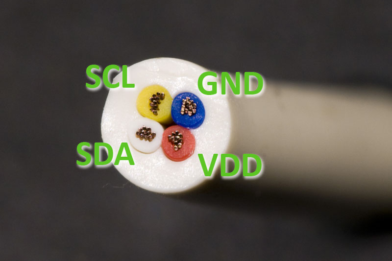
Here is a photo of the cross section of the simple telephone cable used in the experiments in this article. The labels show the initial signal assignment that were used to provide both power and an I2C bus to a temperature sensor.
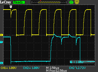
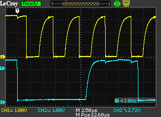
4.7 kohm were used as pull-up resistors. Below is a scope plot of the resulting signals when using 70 cm of cable and a data rate of approximately 200 kHz.
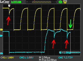
The red arrows show where one signal is disturbed by a fast transition from high to low on the other signal. The green arrow shows that no disturbance can be seen on SCL when SCL is low, despite the fast transition from high to low on SDA. The reason that the signals are only disturbed while they are high is that in the high state, it is only a relatively weak pull-up resistor that keeps the signal at its proper level, so a small amount of current injected into the signal can change the voltage quite a bit. When an I2C signal is low, it is held low by a strong transistor which has an on-resistance of only a few tens of ohms so it would require a current that is two orders of magnitude stronger to cause a disturbance of the same amplitude on a low I2C signal than on a signal in the high state.
If the negative going glitches caused by the crosstalk become large enough, they may cause the bus to fail in various ways as the signals are misinterpreted, so it is important to keep these under control. The I2C specification defines valid high logic levels as being at least 70% of VDD. 70% of 3.3 V is 2.31 V and the glitches in the plot above dip down to this level, which is bad.
Coupling mechanism
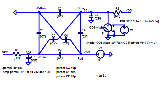
The mechanism for coupling from the disturbing signal (the aggressor) to the disturbed signal (the victim) is the capacitance between the wires in the cable. A schematic model of the I2C-bus and cable (drawn using LTspice) is shown below.
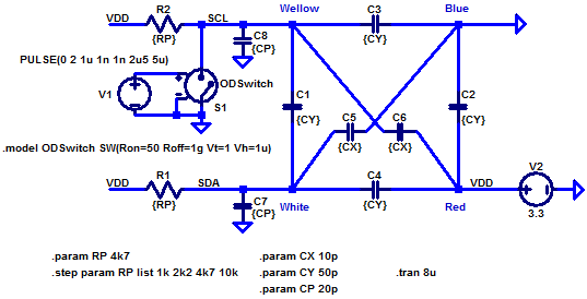
R1 and R2 are the I2C pull-up resistors. C1-C4 are the capacitances between adjacent wires in the cable while C5 and C6 are the capacitances between the diagonal wires. C7 and C8 are stray capacitances on the PCBs as well as capacitances at the pins of the ICs. S1 is a switch that models the open-drain output of the driving pin while V1 controls when the switch is closed and when it is open. The values of several of the components are set as parameters (within curly braces) to make it easier to modify them and adapt them to the actual values of a specific instance of the circuit. The capacitances shown in the schematic are reasonably representative of the real circuit discussed above.
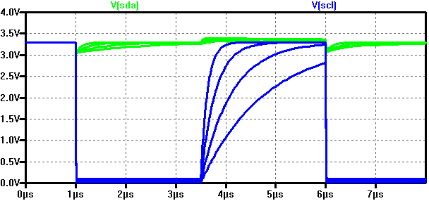
Below are the simulated waveforms of the SCL and SDA signals when the I2C pull-up resistors are stepped from 1k via 2k2 and 4k7 to 10kohms.
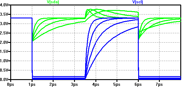
One can note that the amplitude of the glitches and the steepness of the edges match the measurement pretty well for the 4k7 pull-up resistor (the next slowest traces). This supports that the model is fairly accurate.
We can see that the initial glitch in the SDA waveform has (almost) the same amplitude regardless of the the value of the pull-up resistors. This might not be expected, but is a consequence of the fact that the initial part of the step is dominated by the capacitive voltage division in the circuit. The capacitive divider consists of C1 which injects charge into the parallel combination of C4, C5 and C7. Right after the step, the voltages on the capacitors start to recover and how quickly this happens is determined by the value of the pull-up resistor, so the 1k resistor gives a ten times quicker recovery than the 10k resistor. But note that it does not significantly reduce the magnitude of the glitch.
There is also a little crosstalk happening during the slower positive edge of the aggressor. This crosstalk is much less of a problem since it has a positive amplitude and thus either increases the already positive amplitude of the victim signal or does not affect a low victim signal since that is actively being pulled low and is thus almost immune to the disturbance.
Reduced pull-up resistances
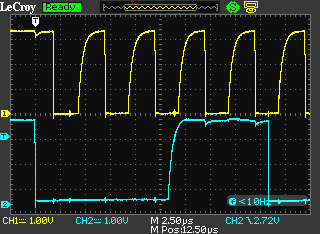
A lower value of the pull-up resistors did not seem to do much good according to the simulation, but let’s anyway verify this in reality. Below is the same measurement as before, but with 2.2 kohm pull-up resistors.
As predicted by the simulation, the amplitude of the glitches remain the same, while the positive edges have become steeper.
Modified cable configuration
So, we could not reduce the amplitude of the crosstalk by the old standard trick of reducing the pull-up resistance. So is there something else that we can try?
Since the coupling mechanism is capacitive, we would like to reduce the capacitance between the aggressor and victim. This can actually be done without changing cables if we change which wire is used for what signal. To do this, the I2C signals are put on diagonal instead of adjacent wires as follows:

(If it had instead been a four-wire ribbon cable, putting the I2C signals on the outer wires and power and GND on the two inner had been the way to go. In a twisted-pair cable, the I2C signals should be twisted with power or GND and absolutely not with each other.)
The resulting crosstalk is shown in the plots below for 4.7k and 2.2k pull-ups.

As can be seen, the glitches have been substantially reduced and are now harmless. This can also be simulated by just changing the simulation schematic slightly to move the aggressor diagonally from the victim:
The resulting waveforms are shown below.
The simulation matches the measurement well also in this case.
So the method of placing the I2C signals far away from each other in the cable is apparently effective, just as expected.
A less elegant possibility is to add more capacitance between the I2C signals and GND, provided the bus capacitance is not already too large. This will affect the capacitive voltage division in a positive manner and reduce the crosstalk by increasing the capacitance from victim to GND instead of reducing the capacitance between aggressor and victim. The cable reassignment above actually did both reduce the aggressor-victim capacitance as well as increase the victim-to-GND (and power) capacitance, so it made use of both mechanisms.
Cable length influence
Another question is how the length of the cable affects the crosstalk. By examining the schematic models of the cables, one can realize that all the cable capacitances (C1-C6) are proportional to the length of the cable. As mentioned above, the amplitude of the crosstalk is controlled by capacitive voltage division. All of the capacitances involved in the division, except for the small external capacitances to GND (C7 and C8), grow linearly with the length of the cable, so as long as the cable capacitances dominate over the stray capacitances to GND, the length of the cable should have only a very minor impact on the amplitude of the crosstalk.
Below is an oscilloscope plot of an I2C bus that is run through 2.7 m of cable.
As expected, the amplitude of the crosstalk has remained essentially the same while the edges are less steep due to the added capacitance.
Summary and recommendations
- I2C is particularly sensitive to capacitive crosstalk since the signals are often not driven by strong drivers, but instead by weak pull-up resistors.
- Glitches caused by crosstalk can cause an I2C bus to malfunction.
- Cables often have a large capacitance between at least some of the wires.
- Reducing the value of the I2C pull-up resistors does not have any significant effect on the crosstalk and is therefore not an effective way of controlling it.
- I2C signals should be placed in a cable such that they have as little capacitance as possible to aggressor signals, i.e. to signals with fast high-to-low transitions (like other I2C signals).
- Capacitance between I2C wires and power and GND wires help reduce crosstalk (but at the expense of higher bus capacitance, and thus slower transitions and reduced maximum speed for a given value of pull-up resistor).
- In twisted pair cables, the I2C signals should be paired with power or GND wires, not with other I2C signals.
- In ribbon cables, the I2C signals should only be adjacent to power or GND wires.
- The length of the cable does normally not affect the amplitude of the crosstalk very much. (As long as the cable is long enough so that the cable capacitance dominates over other bus capacitances.)
- Longer cables do of course add more capacitance and thus reduce the steepness of the positive edges, which can reduce the maximum speed and/or require reduced pull-up resistances.
- It is a very good idea to use an oscilloscope to take a look at the I2C signals in any new design to see if they look good or need to be improved.
I hope this article has provided some intuition about – and insight into – I2C crosstalk in cables and what to do to control it.
But there is problem when we attach more number of slave in i2c, only few work properly. I am using i2c and, I am able to send data over 100 meter but I attached 40 slave and the problem is that only 7 slave working after that program stucked and no other slave is working. Can u help me?
use i2c cable extender p82b715
Hi Markandey,
Sounds like you have a lot of capacitance on the I2C bus. I2C is not really meant to be used with more than 400 pF on each signal and 100 m of cable is likely to have more capacitance than that. Have you looked at the waveforms using an oscilloscope to see if they are degraded?
Possible ways forward are:
– Use a cable with less capacitance. Maybe use a flat modular cable (like http://www.digikey.com/product-detail/en/assmann-wsw-components/AT-K-26-6-B-1000/A0062R-1000-ND/1972592) or a ribbon cable and use the respective outer wires on each side for SCL and SDA while leaving at least the next wire inside unconnected and then having a GND or VCC wire inside of that. E.g. SCL-NC-GND-VCC-NC-SDA (where NC is a non-connected wire). This reduces capacitance and crosstalk within the cable, but increases susceptibility to external EMI due to the wider separation of signals and return paths.
– The high capacitance could perhaps be somewhat managed by reducing the values of the pull-up resistors.
– Use one or more I2C repeater/redriver circuits like e.g. http://www.digikey.com/product-detail/en/nxp-semiconductors/PCA9617ADPJ/568-10211-1-ND/3991867 to extend the range.
– Use the slowest I2C speed possible (100 kbps instead of 400 kbps).
– With 100 m of cable you might even have resistive drop in the cable that reduces your swing too much. Again look at the signals with an oscilloscope (at both ends of the cable). A redriver might be of help also if this is the case.
– Consider using a protocol that is more suitable for 100 m distances, like RS422 or RS485. If you need to use the same I2C slaves you will probably need a microcontroller on each end of the cable to translate between RS422/485 and I2C. The software of your existing controller probably needs to change to accommodate the changes.
Good luck!
Per
We can use P82B96 to:
– convert bidirectional I2C signals into unidirectional
– level translated to up to 12V
– bus capacitance of up to 4000pF
– & use RS-4xx differential drivers & receivers or LVDS driver/receiver pair
Using P82B96 is simple & relatively more robust than using MCU for converting I2C into RS-4xx signal.
I was not aware of that chip, but it looks to be a good and robust solution in many situations where an I2C bus needs to go far. 20 m is mentioned in the datasheet as a distance easily covered by this solution.
I2C is not intended to be used with cables.
As the name implies it is used for Inter Ic Communication on PCB’s.
Anders J
Sure, but it is often quite convenient to be able to use it in cables as well and as I showed in the blog post, this is quite possible if one is careful to minimize capacitive crosstalk to the I2C signals.
In fact, I2C is often a very good candidate to be used over (not too long) cables e.g. when interfacing to sensors or slow peripherals and one wants to minimize the number of wires in the cable and/or the complexity of the system. But it does indeed require a good understanding of capacitive crosstalk (or sheer luck) when planning which wires in a cable to allocate for different signals.
Per,
This is brilliant and looks exactly like the waveforms I am seeing as I try to troubleshoot a system I am working on for a customer. However, I have taken the cable out of the equation and cut the traces on the board and rerouted using wires so I could keep SDA and SCL away from each other but I can’t seem to get rid of the cross talk. Any suggestions?
You don’t need to worry about this. Article is totally misleading. For i2c only care about data voltage level at clock rising edge when data is sampled. Otherwise do not care unless they violated Vil min or Vih max which is said to degrade the lifetime of the parts.
Hi Charlie,
Thanks for your kind and insightful refutation of the article. Unfortunately you are wrong.
First of all, the bus failed to work with the amount of crosstalk shown in the first plot and did work fine after rearranging the wires to reduce crosstalk. This shows that this kind of crosstalk can be important in practice.
Second of all, section 3.1.3 of the specification (as linked to in the article) says this:
“The data on the SDA line must be stable during the HIGH period of the clock. The HIGH or LOW state of the data line can only change when the clock signal on the SCL line is LOW (see Figure 4).”
This is violated if SDA changes due to crosstalk at the same time the clock goes low.
So both in practice and according to the standard this kind of crosstalk can be bad.
Regarding exceeding Vih_max and going below Vil_min, this is usually not a problem on most logic inputs if the current is sufficiently limited. The voltage will be limited by ESD diodes clamping the level to a diode drop above Vdd or below Vss. Such diodes usually can take at least a few tens of mA on modern CMOS chips without problem. If you inject too much current however, a parasitic thyristor in the device may turn on and short the supplies, which is typically a very bad thing. This is called latch-up. See, e.g. https://en.wikipedia.org/wiki/Latch-up
Hi Dan,
Are the disturbances occurring when and only when the other I2C signal goes low? Or do they (also?) happen at other times? If so, there seems to be other signals that disturb I2C and just separating SDA and SCL from each other does not help unless it also separates them from the other aggressor.
Does it help if you twist a GND wire together with each of SDA and SCL? If you ground such a “guard” or shield wire both near the beginning and end of the signal wire it should be pretty effective both against any capacitive as well as inductive crosstalk. If you ground it only at one end, it is ineffective against inductive crosstalk, but still effective against capacitive crosstalk.
How do you probe the signals? If you use a standard 10x passive oscilloscope probe with a pigtail GND clip you might be picking up disturbances with the loop area formed by the pigtail, probe tip and the PCB between the ground clip and the probe tip. Even worse is if you do not have the ground clip of each used probe attached to a good ground point near the probe’s tip. You can see if this noise pickup is a problem by reducing the loop area by bringing the pigtail wire closer to the probe tip and PCB. If the interference shown on the scope is reduced by this, the scope is picking up noise that is not really present on the signal you are trying to measure. A way to very effectively reduce the loop area is to solder an uninsulated wire to a GND point near where you want to probe, pull off the hook of the probe to expose the shield of the probe near the tip and wrap the grounded uninsulated wire around the shield. This should reduce the loop area and pickup by one or two orders of magnitude.
Let me know if you solve this conundrum.
Great article, many thanks!
I have one question for you: when the I2C lines are low, the noise produced on the lines seems lower. You argue that this is because of the lower resistance to GND while they are driven low. However, the amplitude of the noise spike should be the same, as it does not depend on the resistance, only on the capacitive coupling. Is the recovery so fast that it is less visible?
Hi Pit,
Good question. It is a simplification to say that the resistance does not matter. If the resistance is low enough, it starts to have an effect since the current injected by a capacitor is limited by the capacitance times the rate of change of voltage (volts per second). The disturbance is then the resistance to ground times this injected current through the capacitor. When the resistance is reasonably high (perhaps on the order of several hundred ohms or more in this case), the actual value of the resistance does not matter for the initial noise amplitude as it is dwarfed by the surrounding stray capacitances if you have a decent length of cable. However, if the resistance is low enough (like it typically is with a fully turned on transistor to GND, maybe ~10-30 ohms) or the capacitances are small enough (like it is if there is no cable and very little other capacitive coupling), the resistances wins out over the capacitances.
It is just if you have a decent amount of unfortunate stray capacitance (like with a long enough improperly wired cable) and resistances with values that are realistic for pull-up resistors that the actual value of the resistance has negligible effect on the initial noise spike amplitude.
Per
Thanks, the article helps indeed !
I was facing this issue with long cables in a project and after reducing the bus frequency I realized that the problem was crosstalk.
Unfortunately I have no margin with the cable, so I need to think a different bus protocol…
Hi Per,
By chance I stumbled on this article in trying to find supporting material for a customer question. The question was why the I2C specification lists minimum fall times for the edges on the serial lines for fast modes and up. The question is answered in a number of places on the web, and the consensus seems that it is to limit interference generated by exceedingly short fall times on the bus. Your article adds crosstalk between SDA and SCL to the picture, so thanks for that insight.
The main question that I have after reading your article, is if the waveforms that you show are within spec on the fall time, for the fast modes and up? (I guess the absence of such a minimum time for the standard mode is for backwards-compatibility reasons.)
Hi Evert-Jan,
I have not checked whether the fall-time of the circuit in the article meet the spec.
In general, it is good for both signal integrity and EMC to not have faster edges than necessary as crosstalk, reflections and EMI are all reduced with lower edge rates. With today’s shrinking transistor geometries, it is very easy to generate very fast edges (way shorter than a nanosecond), so I think it is a good thing that the I2C spec puts a limit to the edge rate. This should reduce the number of chip manufacturers who accidentally make unnecessarily fast I2C outputs which could otherwise cause trouble in many designs.