Den här artikeln publicerades först i QTC nummer 2 2025.
Programkod, filer för kretskortstillverkning och 3D-modeller för den färdiga sändaren finns på https://github.com/per-magnusson/RP2350-Foxoring-Transmitter.
I del 1 av den här tvådelade artikeln [1] beskrevs hur man från en Raspberry Pi Pico 2 (ett billigt litet mikrokontrollerkort) direkt kan skapa häpnadsväckande bra HF-signaler som bara behöver lite filtrering och antennanpassning för att gott och väl duga till en foxoringsändare för 80m-bandet (3,5 – 3,6 MHz). I denna andra del går vi vidare och bygger en hel sändare baserat på tekniken i del 1.
Filter och antennanpassning
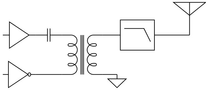
Det behövs en transformator (eller annan balun) för att omvandla den differentiella signalen från processorns pinnar till en ensidig signal som kan matas till sprötantennen. Valet föll på en CX2041ANL från Pulse. Det är en liten ytmonterad 1:1 transformator gjord för 75 ohms impedans och med en förlust på max 0,8 dB i 80m-bandet. Efter omvandlingen sker lämpligen även lågpassfiltrering och någon sorts antennanpassning.
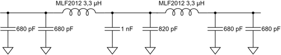
Jag mätte upp utimpedansen från processorn (efter transformatorn) med en nätverksanalysator och fann att den var drygt 100 ohm när båda utgångarna var höga, 90 när en var hög och en låg och 75 när båda var låga. Det vanligaste är att utgångarna har olika nivå, så 90 ohm får anses vara den typiska impedansen. Därför konstruerade jag ett 90-ohms femte ordningens lågpassfilter av chebyshevtyp med ca 4 MHz brytfrekvens. Efter lite itererande med brytfrekvens och rippelnivå i passbandet för att få ett standardvärde på spolarna (3,3 µH) och fint beteende mellan 3,5 och 3,6 MHz även när man simulerar med förlusterna i de valda spolarna, så landade jag i filtret i Figur 1.
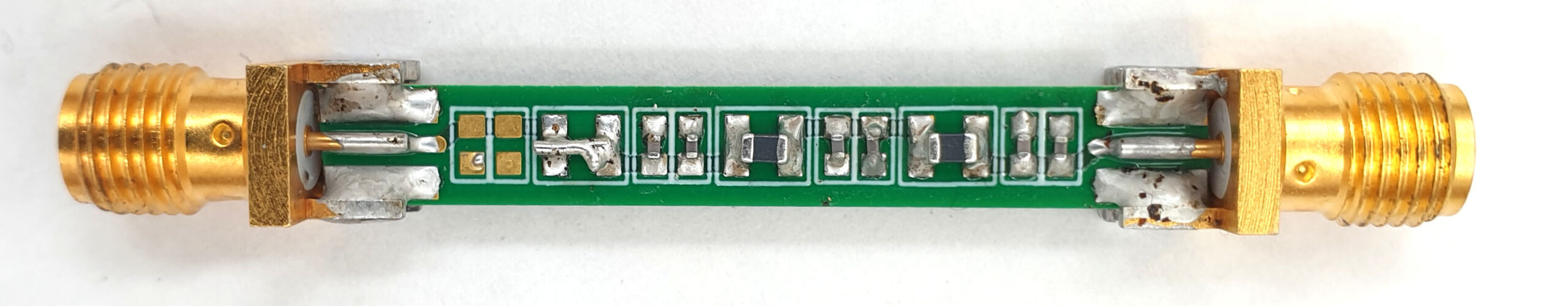
För att testa byggde jag filtret på ett litet filtermönsterkort jag hade liggande, se Figur 2.
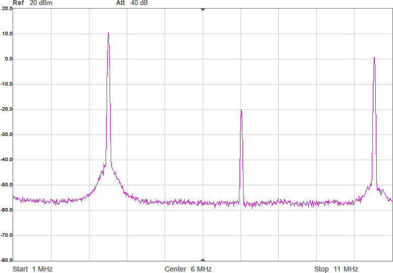
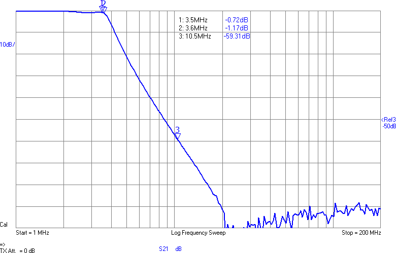
Uppmätt mellan 1 och 200 MHz på en nätverksanalysator (i 50-ohmsomgivning) har det responsen i Figur 3. Dämpningen vid tredje övertonen (10,5 MHz) är nästan 60 dB och förlusten i passbandet runt 1 dB. I verkligheten blir impedanserna som ansluts till filtret annorlunda (speciellt på antennsidan), men den här typen av filter är rätt robusta mot ändringar i omgivningen, så vi borde få vettig filterverkan ändå.
Med 90 ohms utimpedans och en matning till processorn på 3,3 V så kan man räkna ut maximal tillgänglig uteffekt genom att anta att man lastar med matchad impedans, dvs RL = 90 ohm. Toppvärdet över lasten är VP = 3,3/2 V= 1,65 V och max effekt i den är VP2/(2*RL) = 15 mW eller 12 dBm. Förluster i filter och transformatorer är gissningsvis ett par dB så i bästa fall 10 dBm (10 mW) borde i princip vara tillgängligt. Dock har den superkorta antennen (30 cm tänkte jag mig, vilket nog är en typisk antennlängd för en foxoringsändare) minst sagt usel verkningsgrad, så den mängd radioenergi som verkligen sänds ut är i praktiken väldigt mycket lägre. Med någon sorts impedansanpassning mot antennen borde det bli åtminstone signifikant bättre än om antennen kopplas direkt till utgången på filtret. En foxoringsändare ska dessutom inte leverera alltför mycket effekt eftersom det blir för enkelt då, så kanske behöver vi i slutändan dämpa signalen.
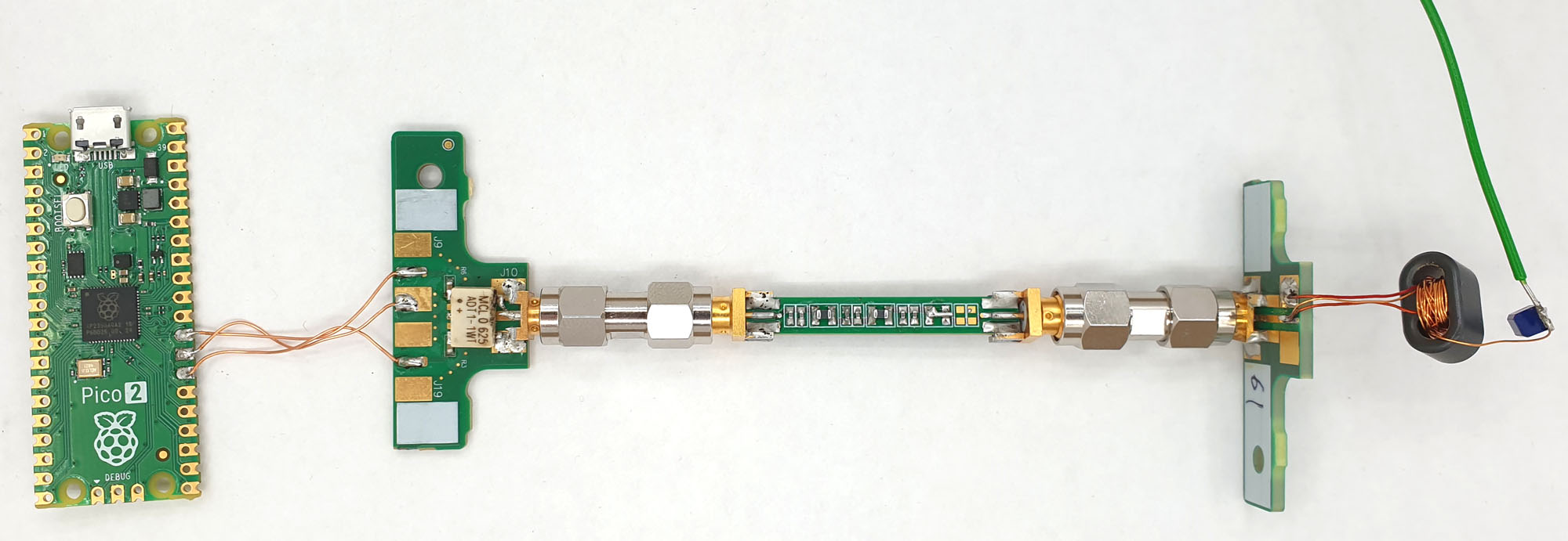
För att få ett relativt mått på effektiviteten hos olika anpassningar byggde jag en enkel testfixtur där sändarantennen hålls på 10 cm avstånd från en 30 cm lång mottagarantenn. Antennerna kopplas till de två portarna på en nätverksanalysator av typen VNWA och en överföringsfunktion, såväl som impedansen hos (den matchade) antennen kan därmed mätas upp. Se Figur 4.
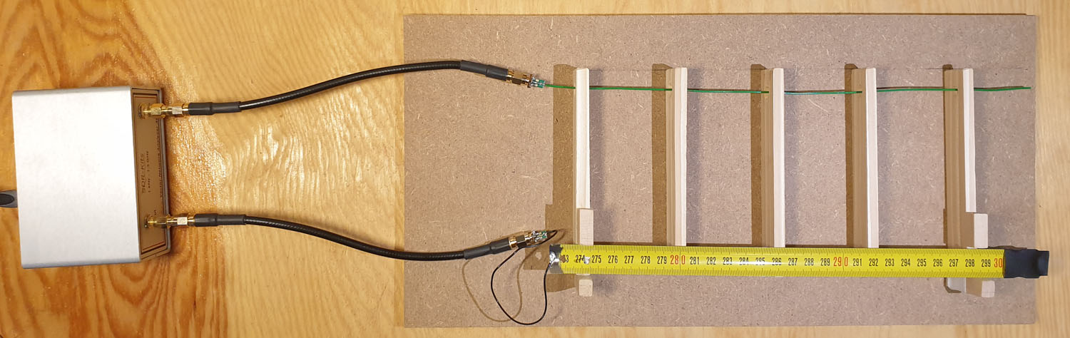
Det går att kritisera uppställningen på flera sätt: Mätningen sker i extremt närfält; mottagarantennens närvaro påverkar sändarantennens impedans en aning; omgivningen är inte kontrollerad eftersom det finns metall, elledningar och störande datorer i närheten; kablar och nätverksanalysator fungerar som motvikt/jordplan till antennen och har inte samma elektromagnetiska egenskaper som den batteridrivna foxoringsändaren som antennen ska kopplas till; det finns visst utrymme för att antennerna rör sig något mellan mätningarna, etc. Men trots alla brister bör bättre överföring mellan sändar- och mottagarantenn för en viss antennanpassning i denna fixtur ändå med stor sannolikhet innebära bättre funktion även i slutapplikationen. Speciellt om skillnaderna är markanta.
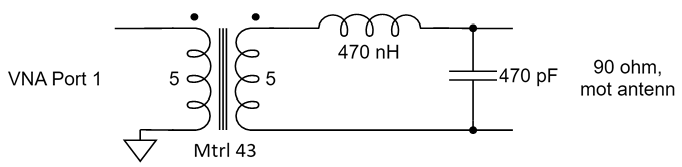
Efter en hel del arbete med att få till en bra antennanpassning med hjälp av mätningar i denna fixtur så insåg jag att den nog ändå inte var tillräckligt bra. Största felet är det där med att koaxkabeln på TX-porten tillsammans med VNA och USB-kabel fungerar som ett jordplan till antennen, vilket förbättrar dess effektivitet markant. Motsvarande kommer ju inte att finnas när det bara är ett litet batteridrivet kretskort som sitter i änden av antennen. För att avhjälpa detta lindade jag en transformator (un-un) på två Fair-Rite-toroider av material 43 och kopplade lindningarna till varsin SMA-kontakt. Lindningarna har 5 varv på vardera primär- och sekundärsidan och är placerade så långt från varandra som möjligt för att minimera kapacitansen. Minimal common-mode-koppling är alltså vad vi är ute efter så att inte kabeln till VNA:n kan fungera som jordplan till antennen. Lindningsinduktansen blev 19,5 µH och läckinduktansen 1,5 µH. 43 är ett material med rätt mycket förluster vid 3,5 MHz, men dämpningen är ändå bara 0,8 dB genom transformatorn i en 50-ohmsomgivning, så det får duga.
När ena sidan av transformatorn termineras med 50 ohm så är den komplexa impedansen 45 + i35 ohm på andra sidan vid 3,55 MHz. Eftersom utgången på filtret ska ha runt 90 ohms impedans i passbandet anpassade jag denna impedans till just 90 ohm. Det bör ge så rättvisande mätningar som möjligt mellan antennerna. Att transformera impedanser är ett standardproblem inom RF-elektronik. Ofta gör man det med LC-länkar och exempelvis på [2] finns en lättanvänd kalkylator som fungerar i det här fallet. Det som behövs är 448 nH i serie och 498 pF till jord. Jag valde standardvärdena 470 nH och 470 pF och resultatet blev utmärkt, inom ett par ohm från 90 ohm reell impedans. Schemat för det hela visas i Figur 5.
Men sändaren har ju trots allt ett litet jordplan för antennen, nämligen kretskortets jordplan, så en realistisk modell av det behöver vara med i mätningarna. Eftersom jag redan tillverkat en första version av mönsterkortet så använder jag ett sådant, kopplat till ”jord” på antennsidan av transformatorn. Den modifierade delen av testuppställningen visas i Figur 6.
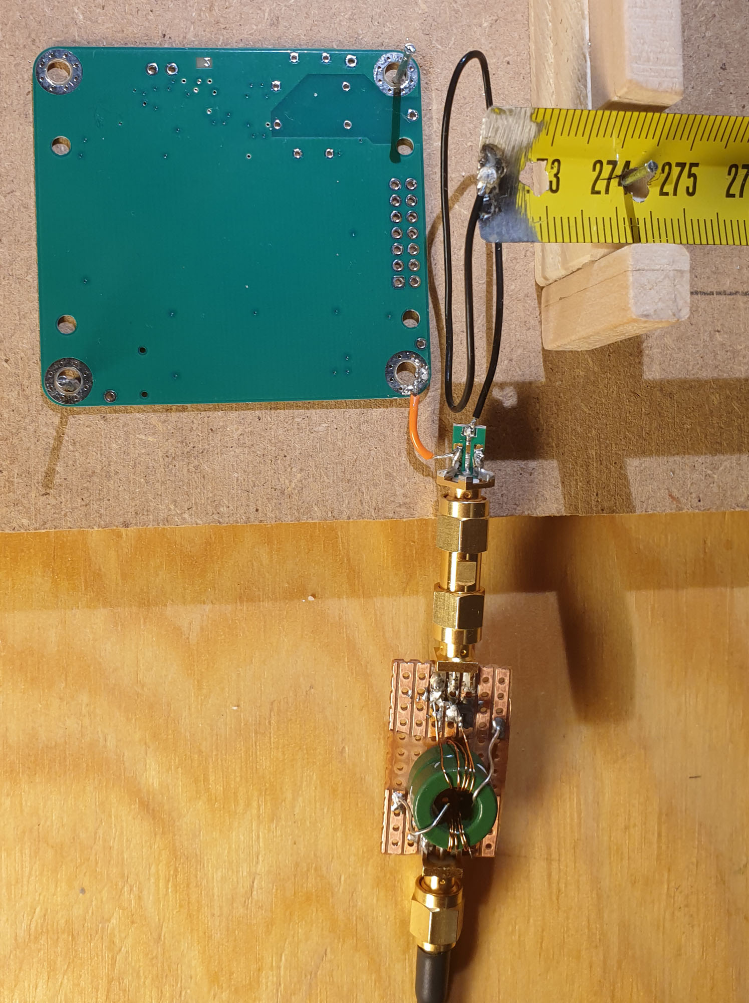
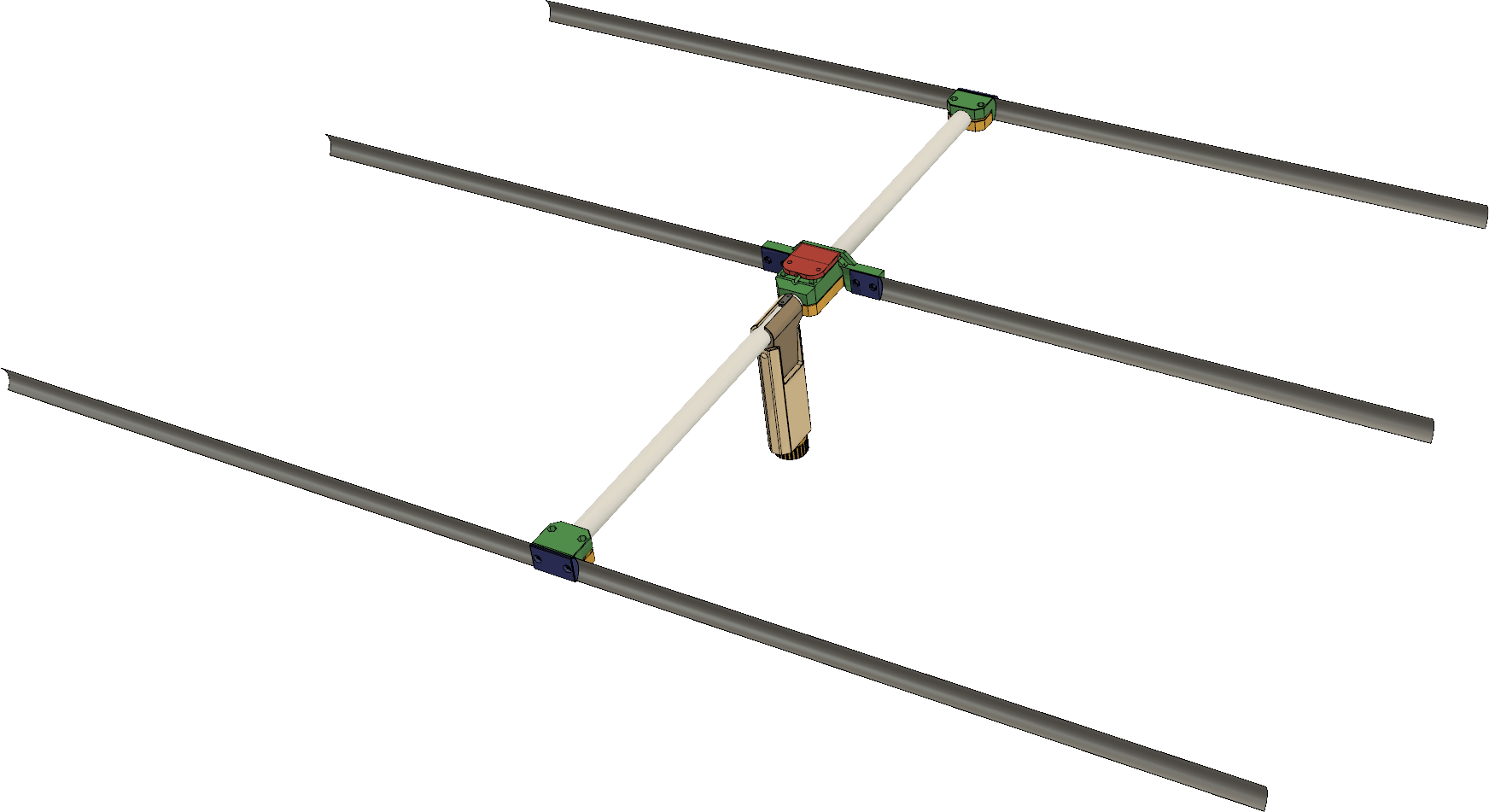
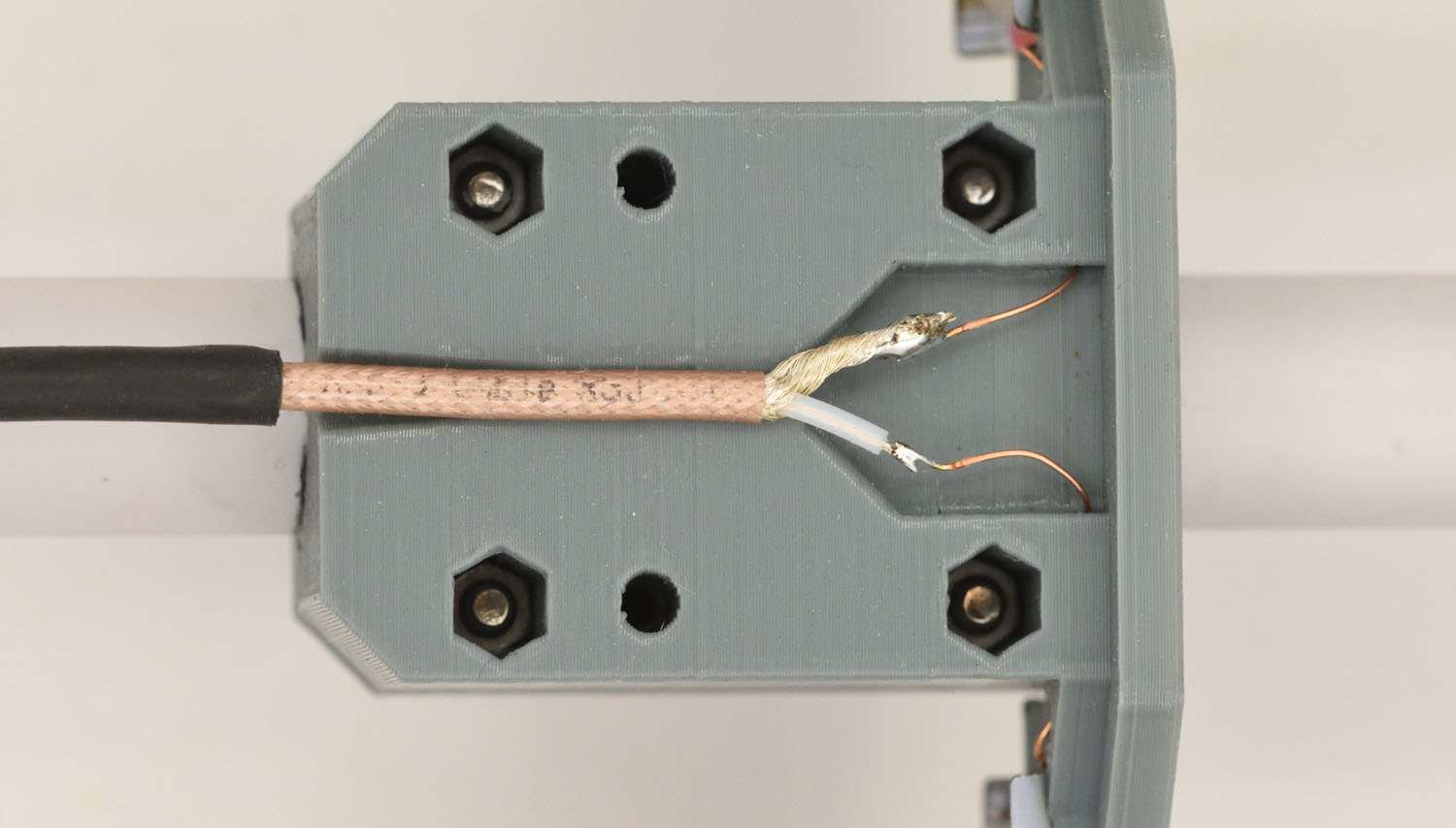
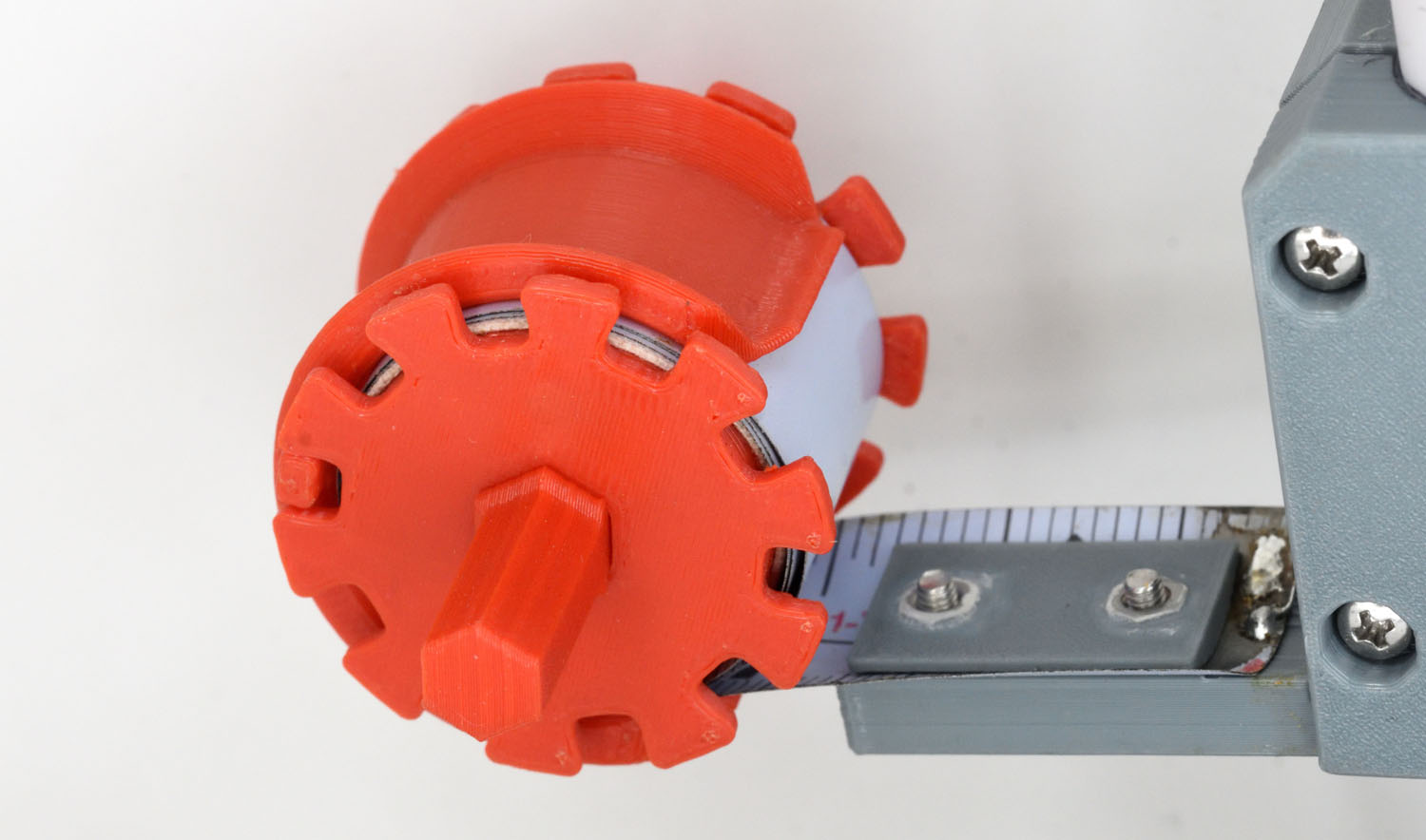
Som sändarantenn valde jag att använda en 30 cm lång bit av ett 19 mm brett stålmåttband (köpt på Jula). Stålmåttband tål att böjas, rätar ut sig av sig själv, är lätt att löda på om man slipar bort färgen och ett billigt 5m-band kostar bara några tior, så det är ett vettigt val för en sådan här antenn. I sändaren kommer det även att behövas en bit kopplingstråd, runt 10 cm lång, för att koppla antennen till kretskortet på ett bekvämt sätt, så en sådan tråd är också med i mätningarna.
VNA:n kan nu kalibreras. Jag valde att ha transformatorn inkopplad vid short-open-load-kalibreringarna så att man ser rättvisande impedanser när man kopplar in något bortom transformatorn, men jag körde utan transformatorn för thru- och thru-match-kalibreringarna.
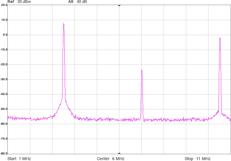
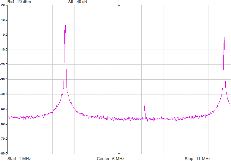
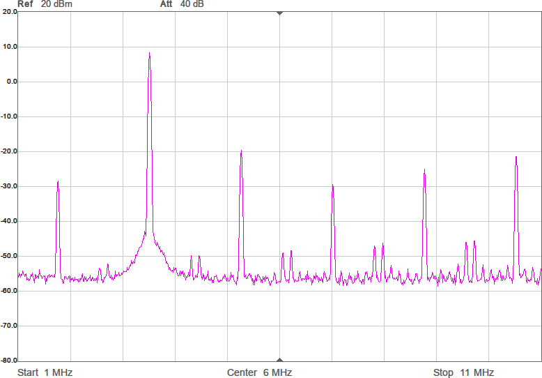
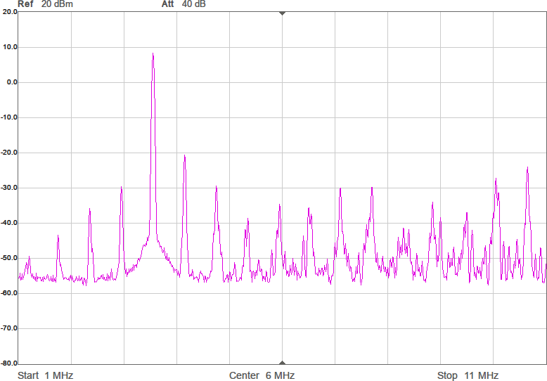
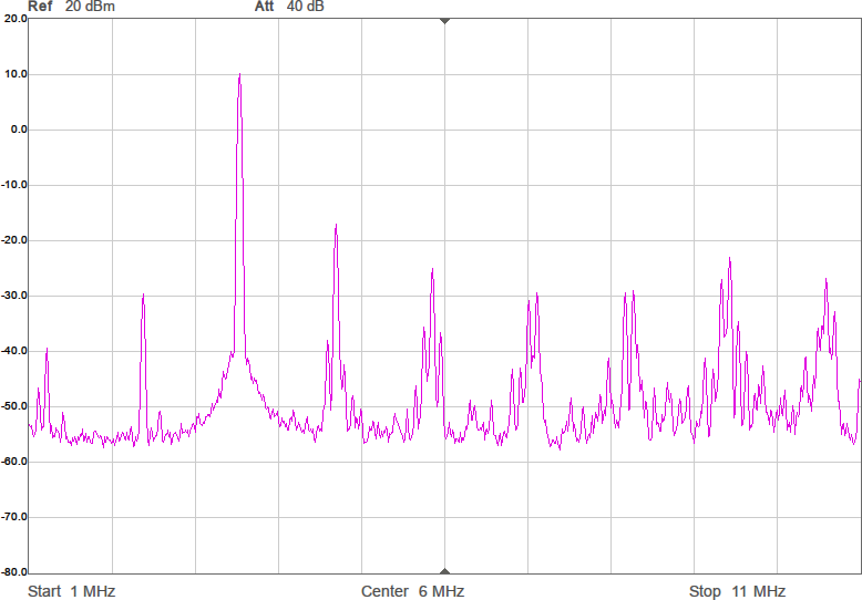
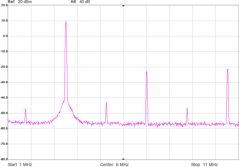
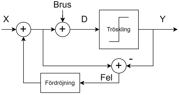
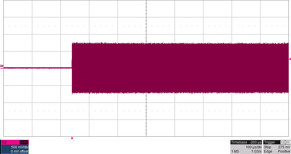
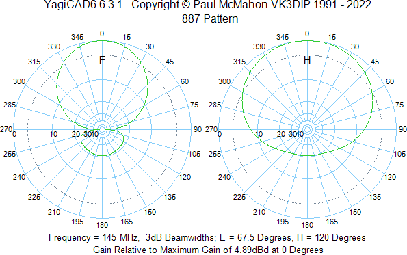
Första mätningen i fixturen blir att ta reda på antennimpedans och överföringsfunktion utan någon anpassning. Se Figur 7.
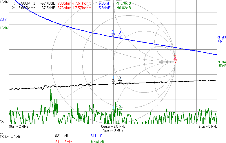
Den svarta kurvan (S21) visar att signalen dämpas 67 dB mellan antennerna. I bakgrunden finns ett Smith-diagram och där ligger alla S11-värden i princip längst till höger, vilket innebär att antennen har (mycket) hög impedans. Smithdiagrammet är som vanligt ritat relativt 50 ohm, så punkten vi egentligen vill matcha mot, 90 ohm, ligger lite till höger om mitten av diagrammet. VNWA-mjukvaran kan omvandla reflektionskoefficienten S11 till komplex impedans (se texten för markörerna högst upp i bilden) och av den framgår att impedansen huvudsakligen är imaginär och negativ, dvs kapacitiv, vilket inte kommer som någon större överraskning. Med tanke på att impedansen är kapacitiv är det även intressant att plotta kapacitans som funktion av frekvens och av den blå kurvan framgår att vid 3,5 MHz ser antennen ut som en kapacitans på 6 pF. Men kapacitansvärdet är väldigt känsligt för placering av t.ex. ledningen mellan SMA-kontakten och antennen. Det är dessutom vanskligt att mäta så här höga impedanser med en VNA som är mest noggrann i närheten av 50 ohm, så det exakta värdet får man ta med en stor nypa salt.
Antennen är alltså väldigt högimpediv och impedansen därför blir känslig för små variationer i omgivningen till antennen. Men vi vill helst ha en robust konstruktion som inte påverkas så mycket av hur kabeln råkar hamna eller om det finns ett träd någon decimeter från antennen.
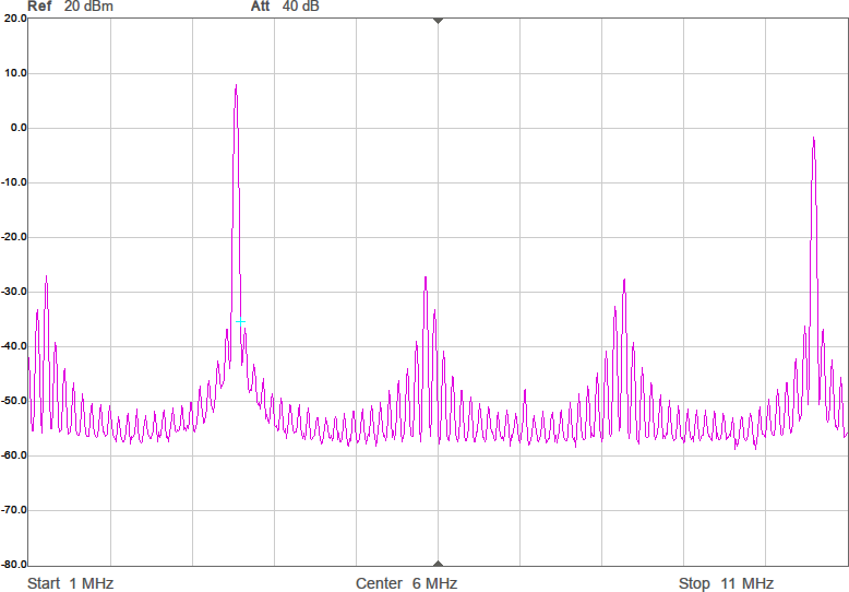
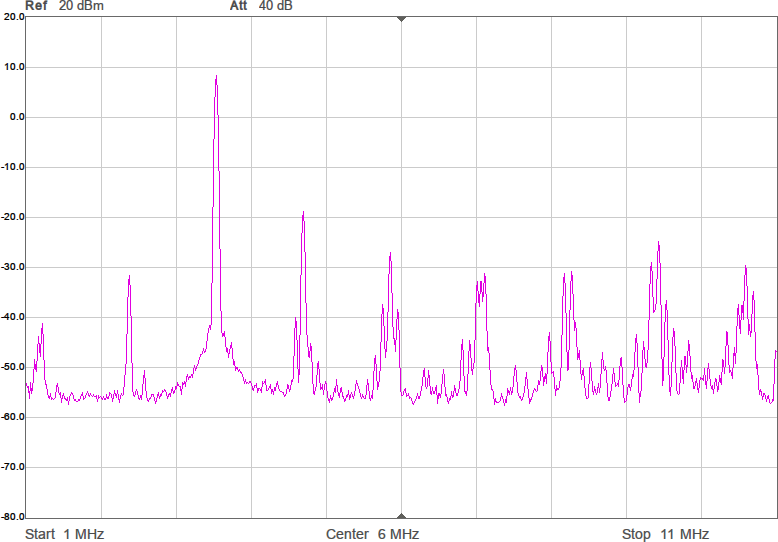
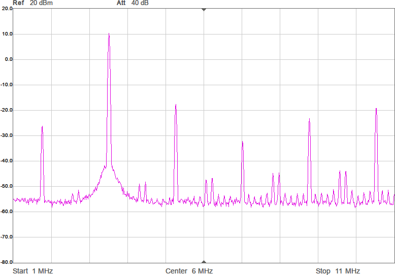
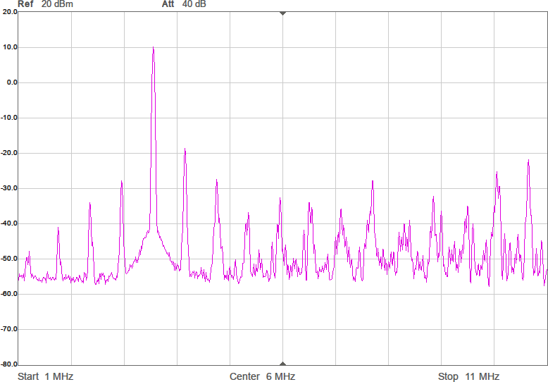
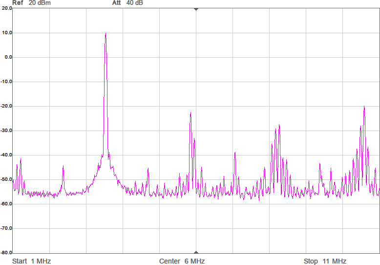
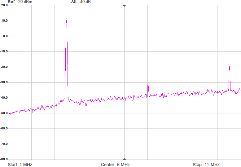
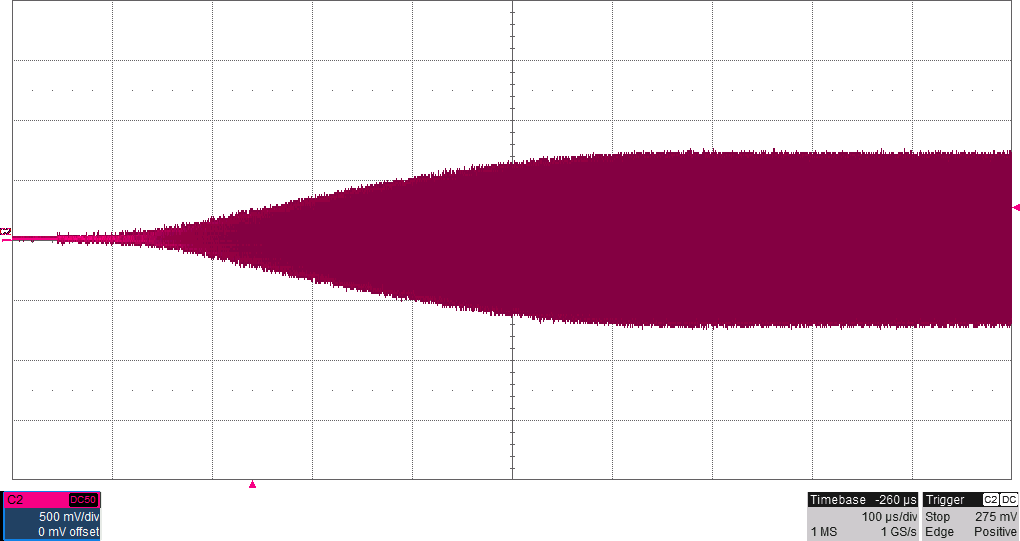
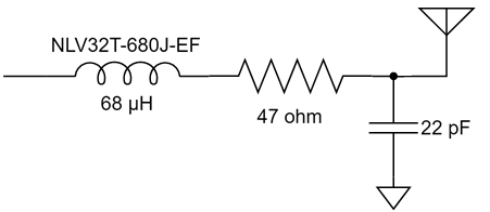
En sak man kan göra för att minska känsligheten är att placera en kondensator parallellt med antennen. Det bör stabilisera impedansen och göra att små ändringar i omgivningen får mindre inverkan. Jag valde 22 pF, vilket bör ge en total kapacitans på runt 28 pF och en reaktiv impedans på -i*1,6 kohm vid 3,5 MHz. Nu skulle vi kunna sätta en spole i serie med denna för att komma i närheten av en reell impedans och för att göra det i trakten av 3,5 MHz behövs 72 µH. Vi testar med standardvärdet 68 µH. Resultatet framgår av Figur 8.
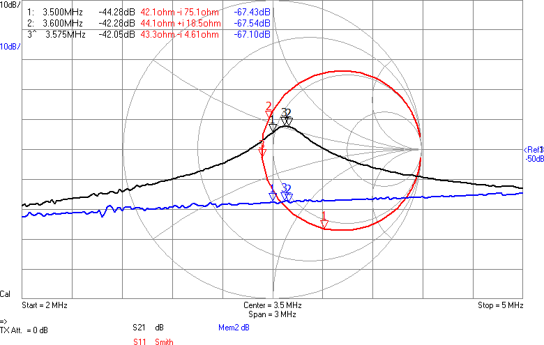
Nu börjar det likna något. Vi har minskat förlusten mellan antennerna med över 23 dB. Det är en förbättring med en faktor 200. Fortfarande är det en bit kvar innan den resistiva delen är 90 ohm, men vi är i alla fall inte mer än en faktor två ifrån. För övrigt lär denna resistans i allt väsentligt utgöras av förluster i spolen, snarare än utstrålad RF-energi.
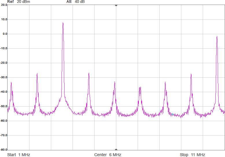
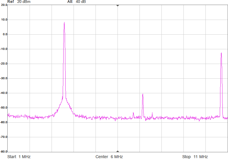
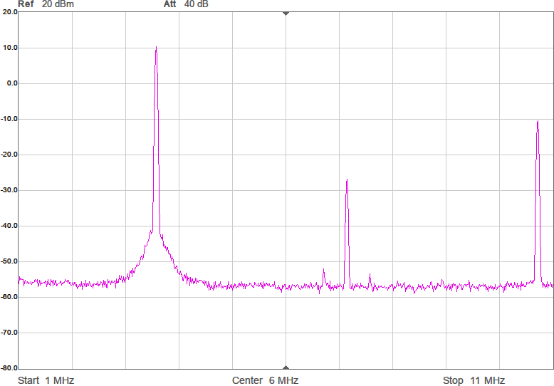
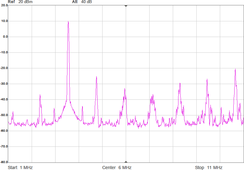
Något man skulle kunna önska är att kurvan vore flackare i bandet så att den frekvens man använder påverkar den utsända effekten mindre. Om vi chansar på att sändaren inte är på gränsen till att vara för svag så skulle man kunna lägga in lite dämpning i form av en resistans i serie med spolen för att minska Q-värdet. Eftersom vi ligger på runt 43 ohm i impedans nu och skulle vilja ligga på 90 ohm för att filtret ska fungera som det är tänkt, åtminstone i passbandet, skulle vi kunna testa med 47 ohm i serie med spolen. Figur 9 visar resultatet.
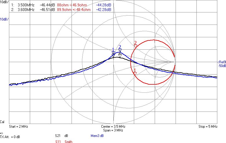
Vi har fått en dämpning på någon dB som väntat, men fördelen är att kurvan är flackare. Möjligen är det även en fördel att vi är nära 90 ohm i bandet. Efter att filtret kopplats in blir det som i Figur 10.
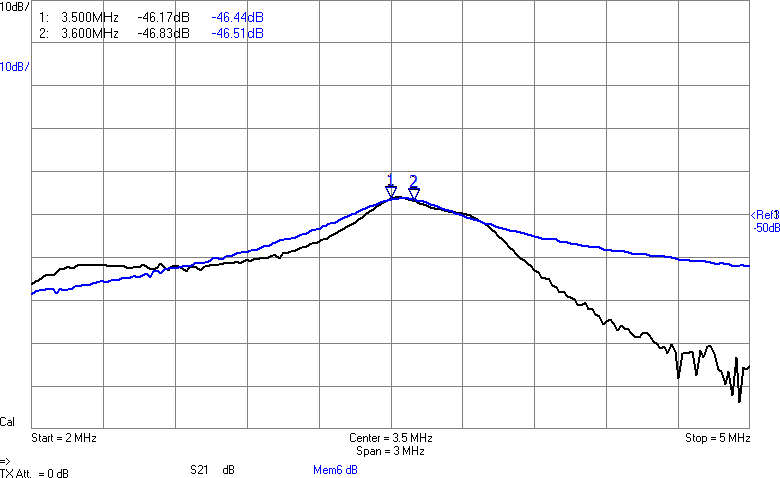
Amplituden har nästan inte påverkats i bandet, men vid högre frekvenser ser man hur filtret gör sitt jobb genom att undertrycka dem. Schemat för anpassningen med dämpning visas i Figur 11.
Frågan är dock om vi får ut tillräckligt starka signaler för en foxoringsändare, så det är dags att testa den detaljen.
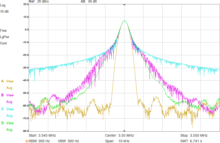
På EM (region-1-mästerskapen) 2024 hade jag en mottagare (en vidareutveckling av [3]) som kan uppskatta avståndet till en sändare genom att man först kalibrerar mottagaren mot sändarens styrka. Baserat på ovetenskapliga tester jag gjort i en skog i närheten dämpas signalen ungefär med 10,5 dB vid en fördubbling av avståndet, så det värdet används i mottagarens beräkning. Det går att spara flera kalibreringar i mottagaren och en av dem jag har kvar är den jag gjorde mot foxoringsändarna på EM, även om de varierade en hel del i hur starka de var. Så genom att rigga upp den nya sändaren och jämföra signalstyrkan på ett visst avstånd med förväntad signalstyrka går det att räkna ut hur mycket starkare eller svagare den nya sändaren är relativt sändarna på EM.
Sagt och gjort. Det visade sig att sändaren är runt 6-8 dB för stark! Anpassningen har kanske lyckats lite väl bra? Men att dämpa är lättare än att förstärka, så det är bara att välja var och hur det ska dämpas. Vi skulle kunna passa på att dela upp dämpningen på ett par olika ställen. Dels skulle man kunna spara lite ström genom att inte lasta processorpinnarna så hårt och dels skulle man kunna dämpa ytterligare nära antennen för att få den än mer bredbandig. Vi ha redan lite dämpning vid antennen, så jag valde att bara dämpa ytterligare vid processorn.
Dämpningen på utgången av processorn bör utnyttjas för att få så hög impedans som möjligt mot processorn så att vi sparar ström, medan 90 ohms impedans behålls mot filtret så att vi slipper designa om det. Här kan man sedan ändra resistansvärden för att justera amplituden utan att samtidigt behöva ändra någon anpassningskomponent. Schemat för dämpningen framgår av Figur 12.
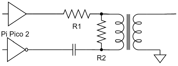
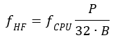
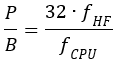
Med hjälp av lite algebra trillar formler ut för R1 och R2 som funktion av önskad ”förstärkning” enligt Figur 13:
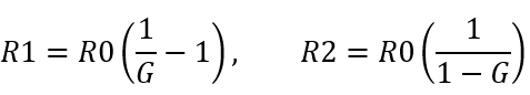
Där G är önskad spänningsförstärkning (mindre än 1) och R0 är utimpedansen på processorn, tillika önskad impedans mot filtret, dvs 90 ohm. Om vi vill dämpa 6,5 dB blir G = 0,47. Det ger R1 = 100 ohm och R2 = 171 ohm. Vi kan välja standardvärdena 100 respektive 180 ohm.
Med denna ytterligare dämpning upplever jag sändaren som ungefär lika stark som de som användes på EM.
Kretskort
Nu är RF-kedjan klar och egentligen skulle det inte behövas så mycket mer elektronik för att få till en komplett foxoringsändare. Men jag ville lyxa till det lite på ett par olika sätt. Dels ville jag ha några omkopplare som man kan använda för att konfigurera sändaren utan att behöva koppla den till en dator och dels ville jag ha en liten display som talar om hur den är konfigurerad och vad batterispänningen är för att lätt kunna säkerställa att allt är i sin ordning inför användning. Tanken är att i normalfallet driva sändaren med tre AA-batterier, men om man får för sig att istället mata den från en power bank är det även praktiskt att ha möjlighet att periodiskt (kanske var 15:e sekund) dra en högre strömpuls för att övertyga strömsparfunktionen i powerbanken om att det visst finns en last inkopplad som fortfarande vill ha matning.
Anledningen till att ha AA-batterier som huvudalternativ framför t.ex. laddningsbara LiPo är för att det är mer kostnadseffektivt och praktiskt. Tre AA-batterier får man för under 10 kr medan ett lämpligt LiPo-batteri skulle kosta ungefär det tiodubbla. Med 2000 mAh kapacitet hos ett alkaliskt AA-batteri och en medelströmförbrukning på under 50 mA så räcker färska batterier i gott och väl ett dygn. För enkelhets skull är programkoden skriven så att sändaren alltid är aktiv när den har matning. Man slår alltså lämpligen på den när man sätter ut den i skogen och slår av den när man hämtar in den. Det här bör ge maximal sannolikhet att sändaren är påslagen när den ska vara det, speciellt om man är noga att kolla batteristatus i displayen innan man ger sig ut. En nackdel är att man inte bör sätta ut sändarna redan dagen innan loppet. Om man antar att det tar sex timmar från att man sätter ut en sändare till att man hämtar in den så räcker en uppsättning batterier med marginal till minst fyra lopp, även om man byter innan de är helt tomma. Det skulle alltså krävas ca 40 arrangemang innan man tjänat in de dyrare LiPo-batterierna. Med AA-batterier slipper man även krånglet med att ladda kanske 10 sändare efter ett lopp. Istället får man byta batterier ibland.
Det kompletta kopplingsschemat visas i Figur 14. Detta är en något förbättrad version mot vad jag själv byggde och innehåller den förenklade antennanpassningen som beskrivits ovan. På korten jag tillverkde finns istället en antennanpassning som även innehåller en transformator.
Jag lade förresten även till en spole (L4) före lågpassfiltret för att inte de högfrekventa komponenterna i sigma-deltasignalen ska se en låg impedans till jord. Detta minskar strömförbrukningen med någon mA. L4 är resonant med DC-blockningskondensatorn C1 före balunen vid ca 3,5 MHz, så den har minimal påverkan på filtret i 80m-bandet. Några ytterligare komponenter för att utöka möjligheterna till andra antennanpassningar finns också med, men monteras inte alls eller med nollohmsmotstånd.
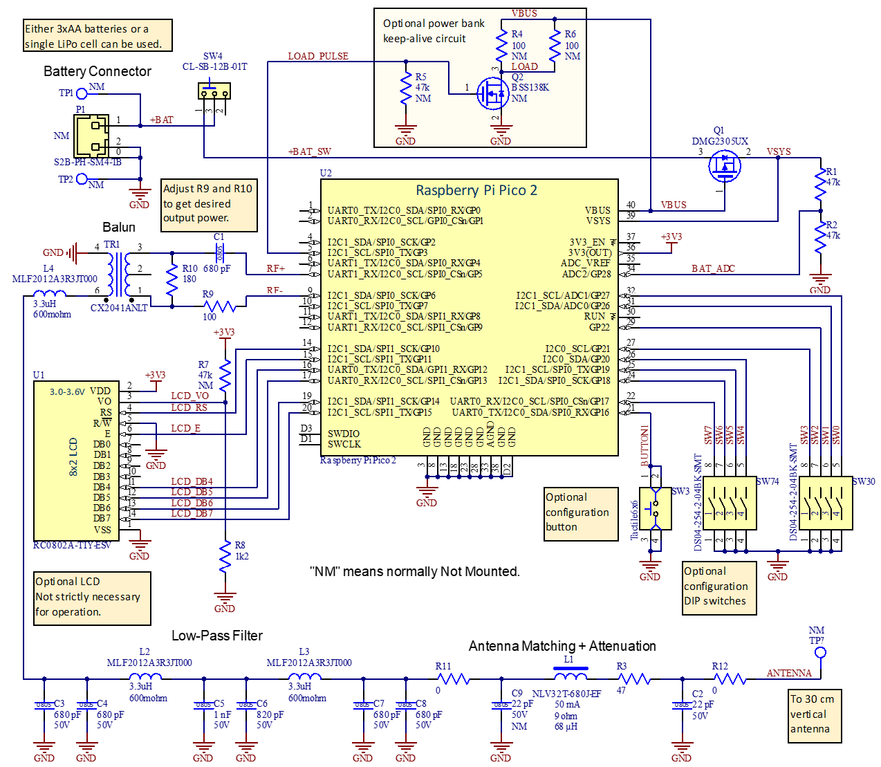
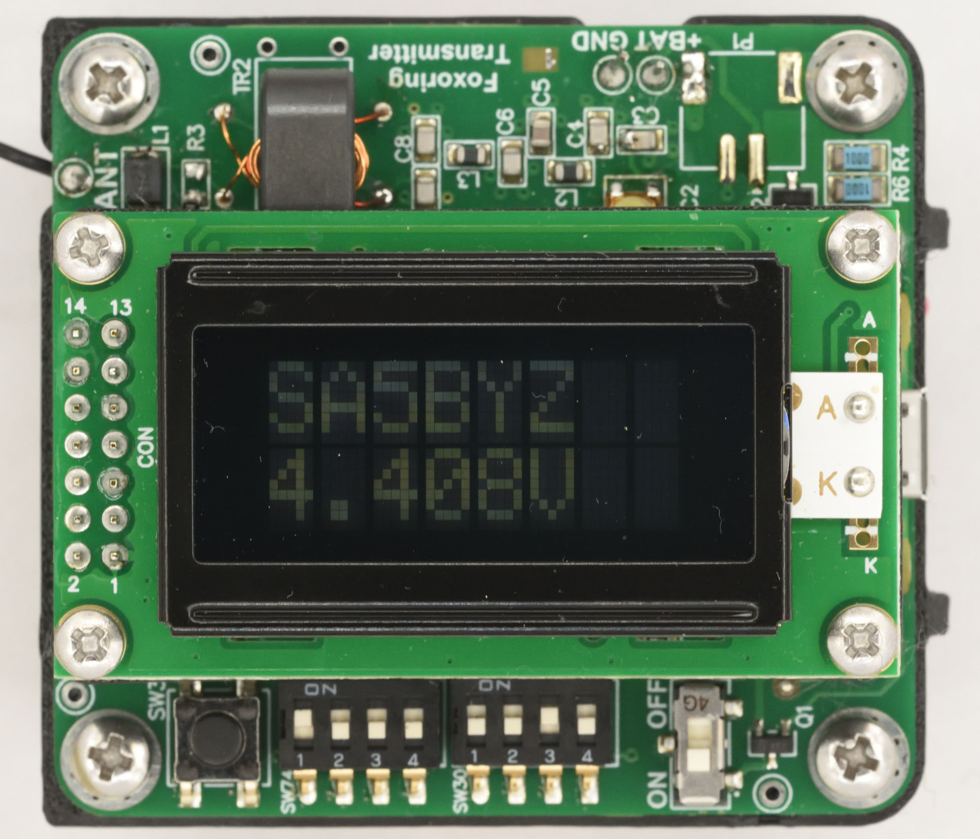
Batterispänningen från en hållare med tre AA-batterier kommer in på TP1 och TP2 (alternativt kan man koppla in ett LiPo-batteri till P1, men det finns ingen inbyggd laddare). Med brytaren SW4 kan man slå av/på sändaren. Inbyggt i processorkortet finns en buck/boost-omvandlare som kan omvandla spänningar mellan 1,8 och 5,5 V till 3,3 V som driver processorn (och LCD:n). Under programmering matas det hela istället via USB-kabeln. Spänningen från USB-porten kommer ut på VBUS och slår av PMOS-transistorn Q1 som då kopplar bort eventuellt batteri. När USB-spänningen inte finns tillgänglig är Q1 påslagen och kopplar in batteripacken till VSYS som är ingången till buck/boost-regulatorn. R1-R2 är en spänningsdelare som gör att processorn kan mäta batterispänningen och visa den på LCD:n.
RF-signalerna kommer ut från processorkortet Pi Pico 2 på GP5 och GP6 och kopplas vidare till RF-kedjan med DC-blockering, dämpare, balun, filter och antennanpassning enligt tidigare beskrivning. Några extra komponenter har lagts till för att möjliggöra mer avancerade antennanpassningar, men monteras inte, eller med nollohmsmotstånd.
Processorn är även ansluten till en liten LCD för statusinformation och några omkopplare för konfigurering. Mer om det längre ned.
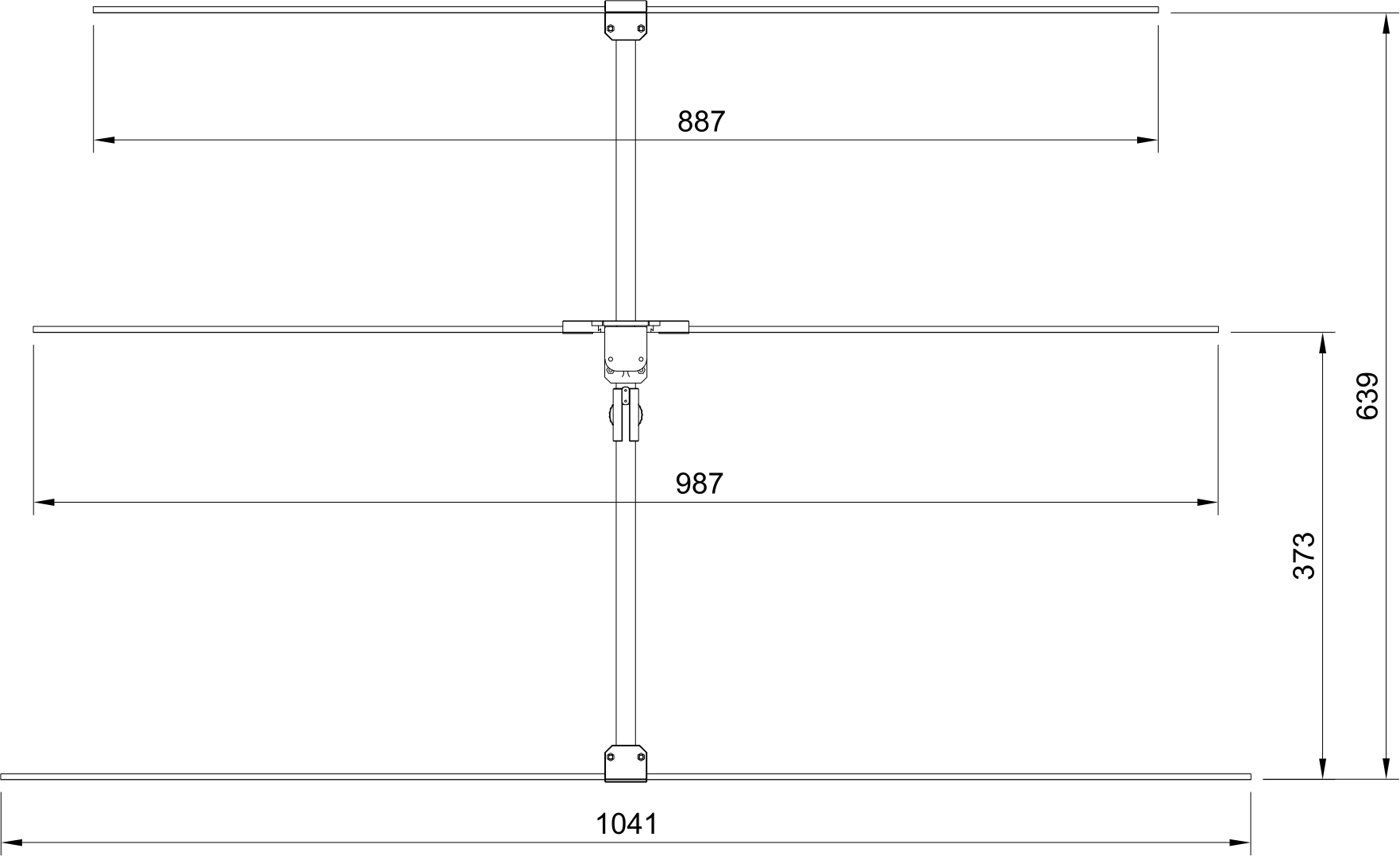
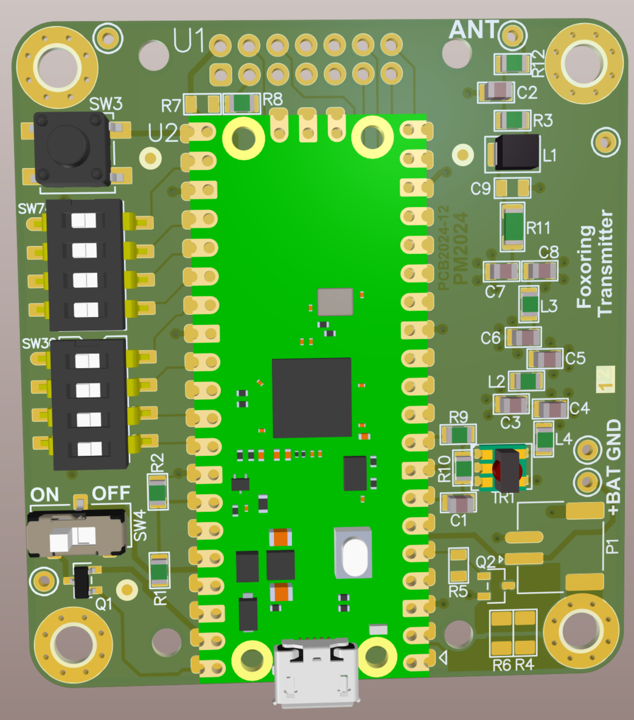
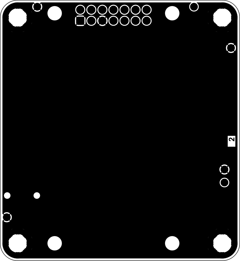
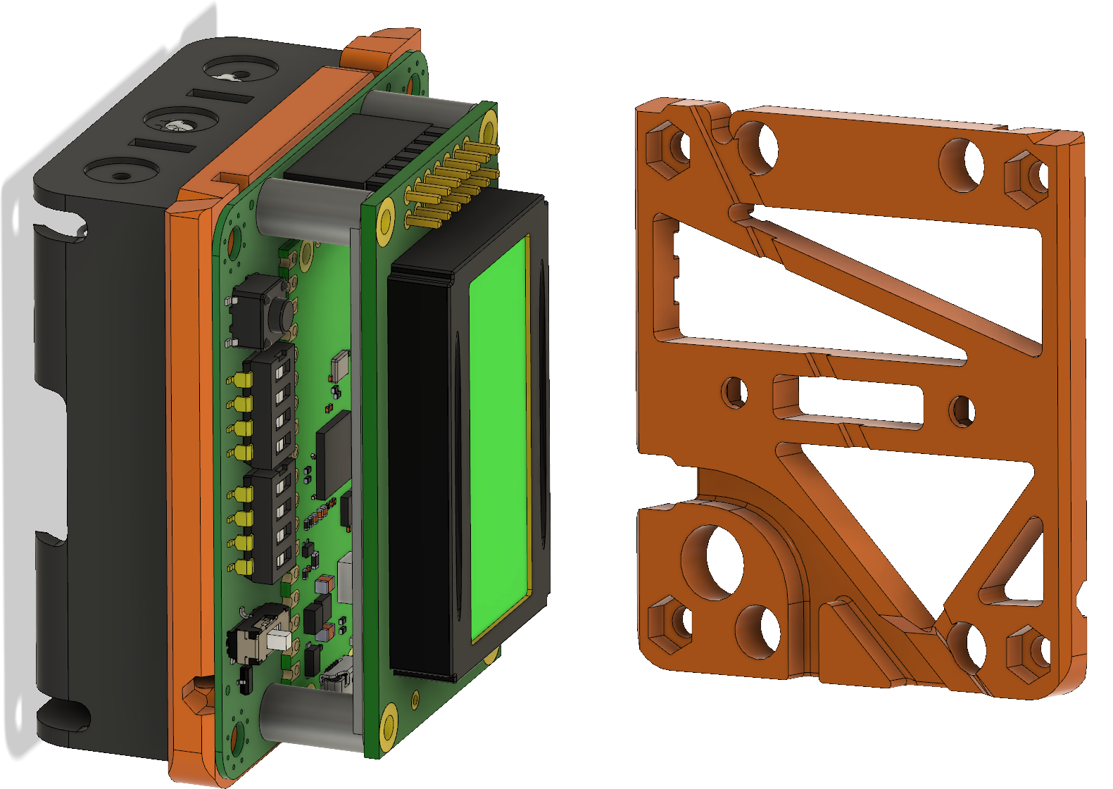
Monteringsritningen och en 3D-vy av kortet (utan LCD eftersom den skulle skymma många detaljer) visas i Figur 15.
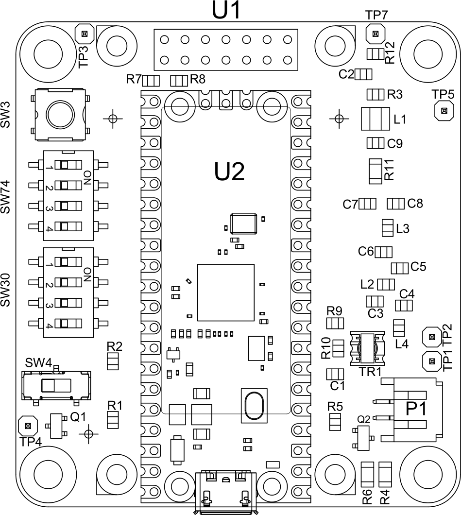
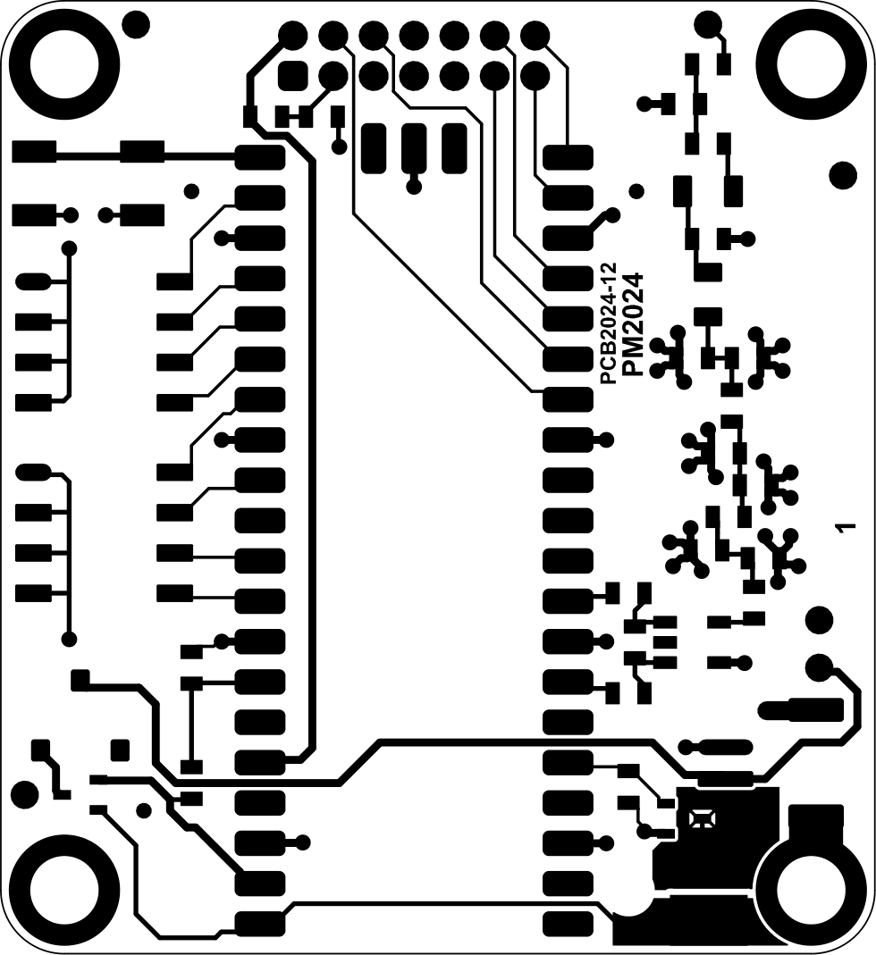
Kortet har två kopparlager, varav det undre enbart är ett jordplan. Alla ledningar gick att dra på ovansidan tack vare ett lämpligt val av vilka processorpinnar som används till vad. De två kopparlagren visas i Figur 16. Eftersom det inte är särskilt många komponenter på kortet och storlekskraven är modesta, så valde jag att använda större ytmonterade komponenter än jag normalt jobbar med. Alla kondensatorer, spolar och motstånd är av storlek 0805 eller större, vilket gör att de är ganska lätta att löda, även om någon form av förstoringshjälpmedel antagligen underlättar.
För att hålla nere den oönskade ströinduktansen hos kondensatorerna i filtret så att dämpningen vid höga frekvenser (100+ MHz) blir stor är kortet 0,8 mm tjockt istället för de vanligare 1,6 mm. Dessutom används fyra vior per kondensator för att ytterligare minska induktansen. Jag beställde 25 kort från JLCPCB och inklusive frakt och andra pålagor var den totala kostnaden drygt 700 kr. Kortets storlek är 55 x 60 mm, vilket bara är aningen större än en batterihållare för tre AA-batterier.
SW30 och SW74 är fyrdubbla DIP-brytare som kan användas för att välja funktion på sändaren. Så som programkoden är skriven för tillfället så väljer SW74 vilken frekvens som ska användas enligt Figur 17.
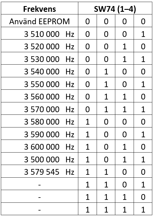
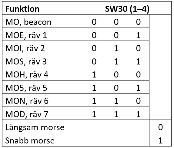
Om SW74 står på 0000 så används inställningarna i det icke-flyktiga minnet (SW30 ignoreras), vilket möjliggör annan frekvens, morsetakt eller morsetecken än man kan ställa in med omkopplarna. Oavsett inställning måste/bör man programmera in vilken anropssignal som ska användas genom att vid något tillfälle koppla upp sig via USB och lagra den i det icke-flyktiga minnet. Om SW74-inställningen är något annat än 0000 så är SW30 aktiv och anger rävnummer och om det ska sändas snabb eller långsam morse enligt Figur 18.
Brytarna läses dels av vid spänningstillslag och dels om man trycker på knappen SW3. Om man vill ha någon annan funktion på brytarna (t.ex. andra frekvenser) är det bara att ändra lite i programvaran. Om man nöjer sig med att ställa in funktionen genom att koppla upp sig med USB-kabel och ett terminalprogram så behövs inga brytare alls. Då gäller inställningen man gjort via kommandon i terminalfönstret och sparat till det icke-flyktiga minnet.
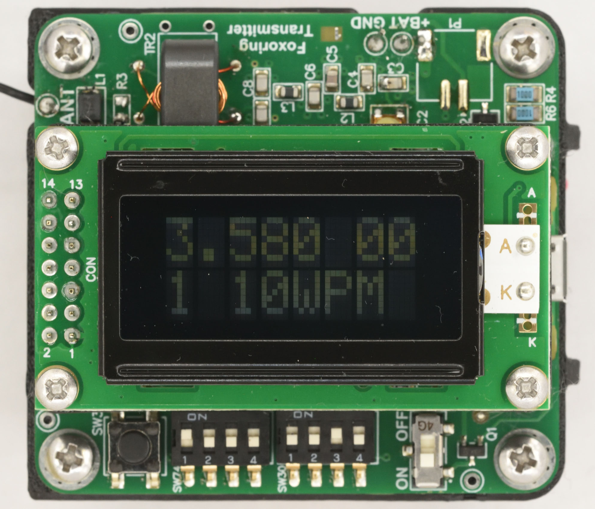
U1 är en liten tvåradig LCD med åtta alfanumeriska tecken per rad. Det var den minsta (och billigaste) alfanumeriska LCD som gick att mata med 3,3 V som jag hittade. Det kändes onödigt att göra sändaren väsentligt större på grund av storleken på en inte helt livsnödvändig LCD, så att hitta något litet var prioriterat. Tyvärr hade den ett fel i databladet som kostade många timmars felsökande. Det stod nämligen att ben 3 inte skulle anslutas, men i själva verket är detta (som på så många andra LCD:er) ett ben som ska kopplas till en spänningsdelare för att ställa in kontrasten på skärmen. När benet är oanslutet syns ingenting på displayen. Till slut visade det sig att det var lämpligt att koppla 1,2 kohm mellan jord och ben 3.
Eftersom LCD:n har så få tecken så växlar den hela tiden mellan att visa olika information. Se Figur 19.
Slutligen utgör Q2 och komponenterna runt den en möjlighet att periodiskt dra korta pulser med mer ström än normalt. Det är användbart om man matar sändaren via en power bank (kopplad till USB-porten) som envisas med att slå av sin utspänning om det inte dragits signifikant med ström på ett tag. Det kan behövas lite experimenterande och ändring i koden för att passa en viss power bank. Om sändaren drivs av batteri snarare än via USB-kabeln gör Q2 ingen skada eftersom en diod på processorkortet isolerar den från batteriet.
Mekanik
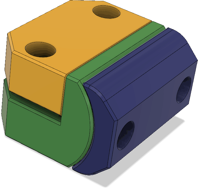
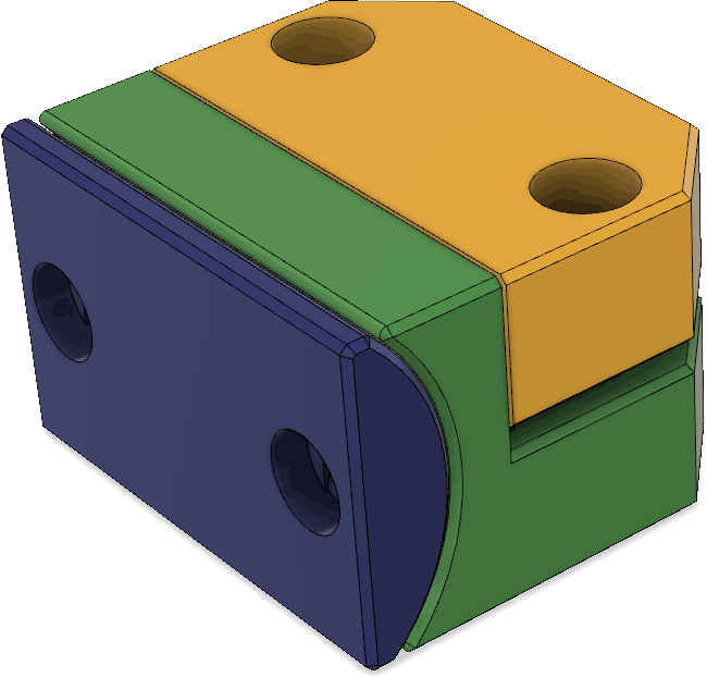
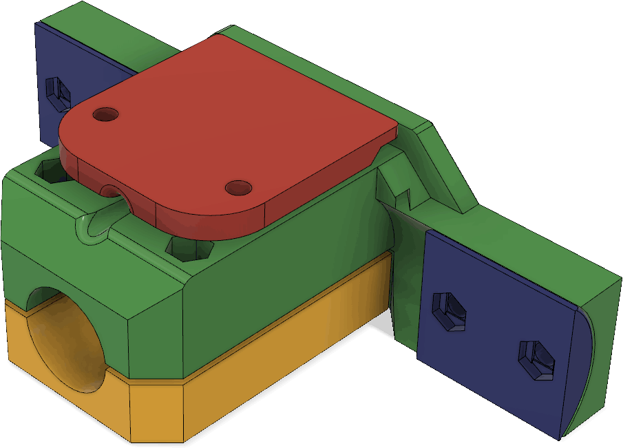
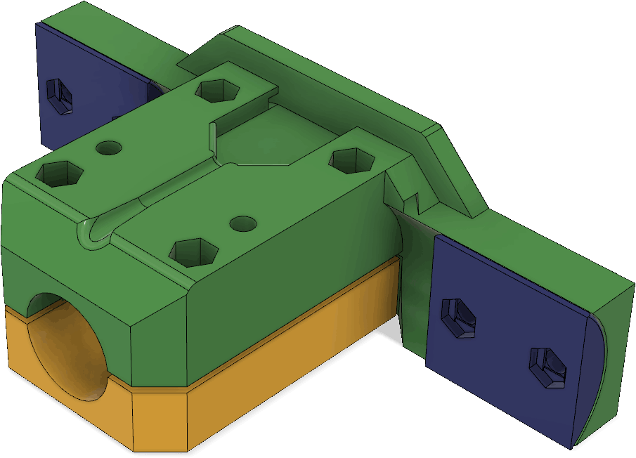
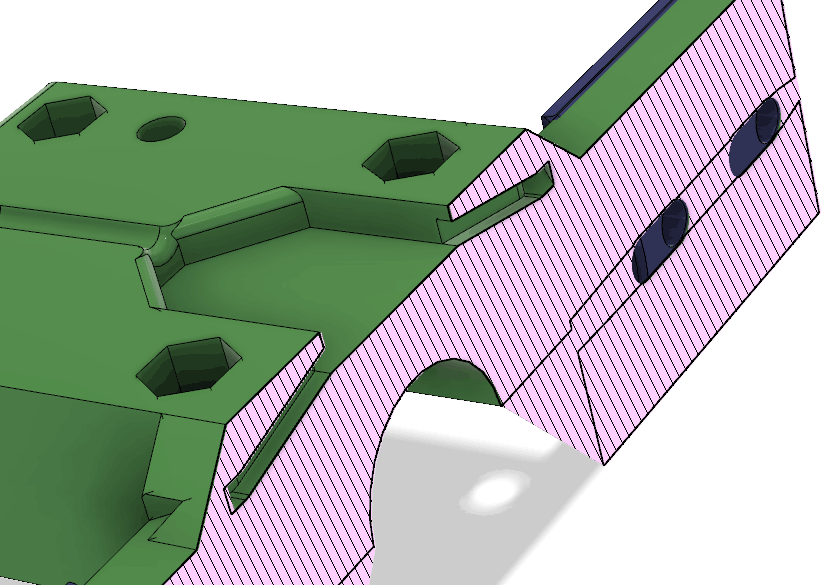
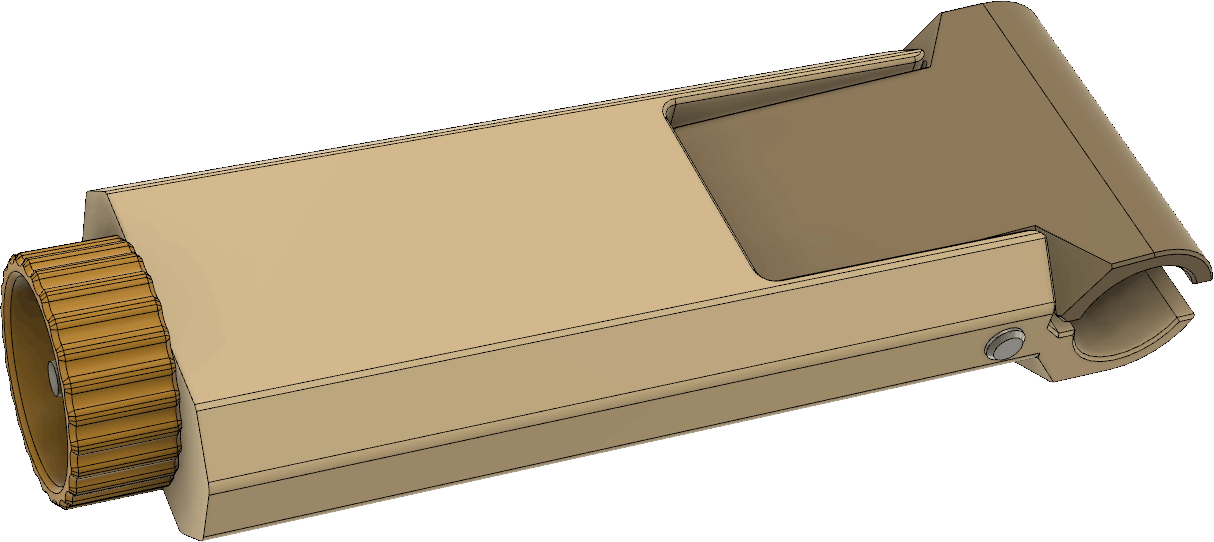
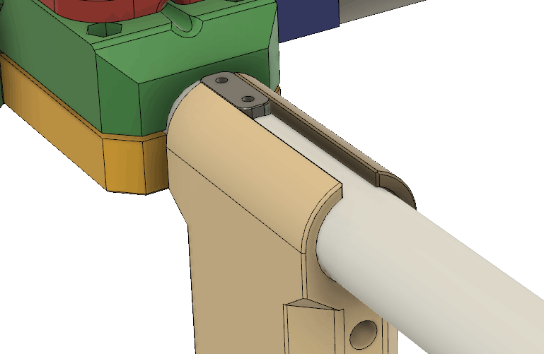
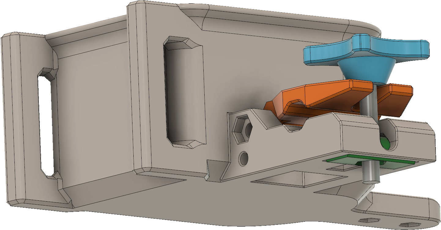
Sändaren behöver såklart byggas in i någon form av låda så att den tål att vara utomhus. En användbar finess vore om det gick att fästa lådan på ett ”glasfiberspjut” av den typ som ofta används på orienteringar för att hålla upp en elektronisk stämplingsenhet. Så brukar man göra på EM/VM och det är praktiskt om man ändå använder sådana spjut för att hålla stämplingsenheten. Eftersom jag har en 3D-skrivare så valde jag att rita ihop en lådkonstruktion som kan skrivas ut på den, vilket sparar in mycket jobb med håltagning och andra modifieringar som skulle behövas om man använde en standardlåda. Batterihållaren och kretskortet fästs på varsin sida av en mellanliggande 3D-utskriven fästplatta, se Figur 20. LCD:n hålls fast med M2,5-skruvar genom 3D-utskrivna distanser ovanför kretskortet. Detta utgör den kompakta kärnan i sändaren och den snäpper in i lådan utan några skruvar. När man vill byta batterier eller koppla in en USB-kabel kan man lätt snäppa ut elektronikpaketet genom att lätt böja ut övre delen av sidoväggarna.
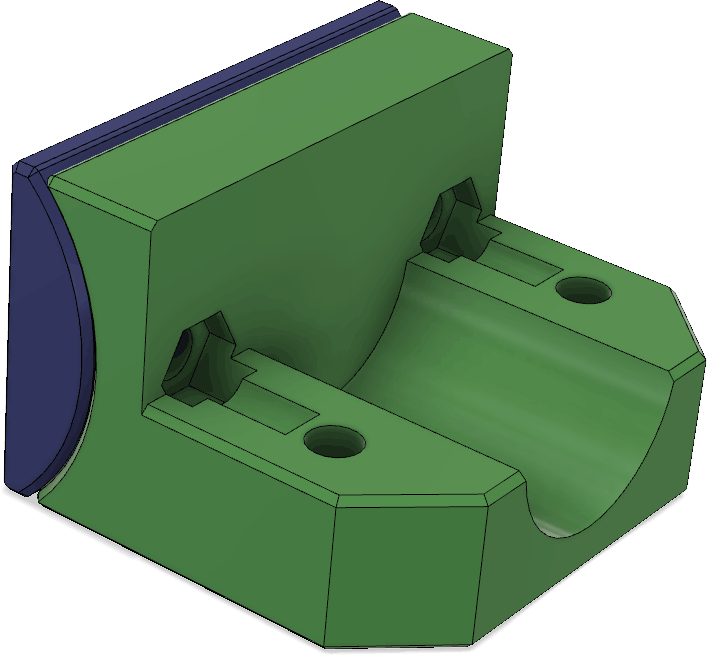
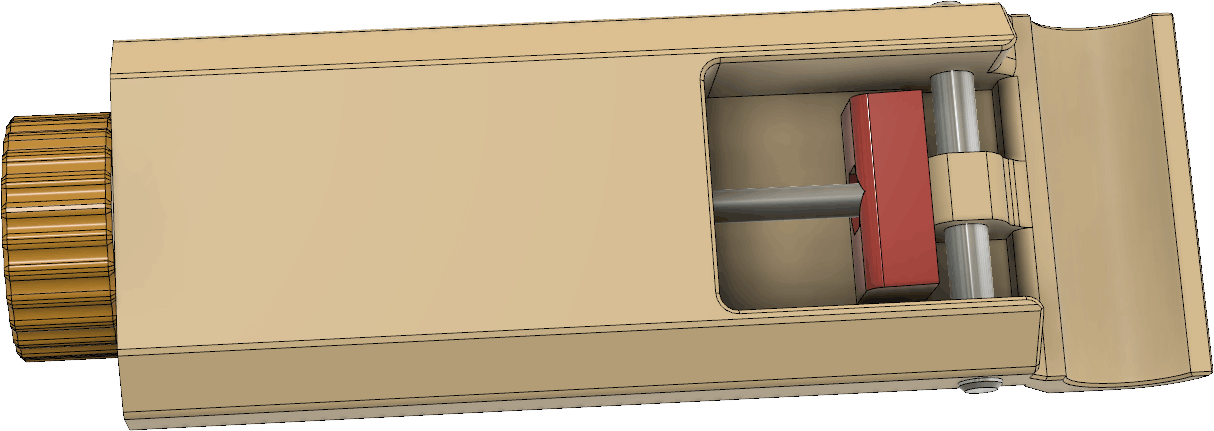
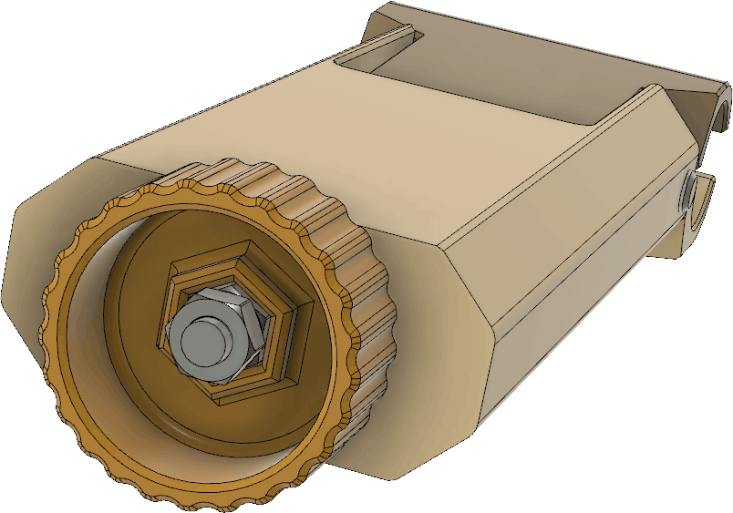
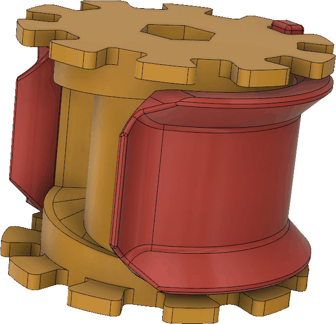
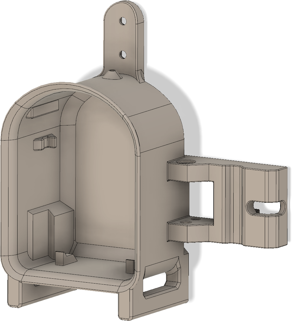
Lådan visas i Figur 21. Hela framsidan är öppen och har utsvängda kanter som dels fungerar som skenor för locket som skjuts på uppifrån och dels förhindrar regnvatten att rinna in. Inuti lådan finns styrklackar nedtill och snäppfästen på sidorna för elektroniken. Till höger finns en utskjutande del som ingår i anordningen för att hålla fast vid glasfiberspjutet. Upptill finns ett fäste för måttbandsantennen samt ett hål för ledningen till antennen. Hålet bör tätas med lim för att inte läcka in vatten. Nedtill finns fötter så att sändaren även kan stå upprätt på ett plant underlag. Fötterna har avlånga hål som man kan vika ned antennen i för att göra sändaren mindre skrymmande under transport.
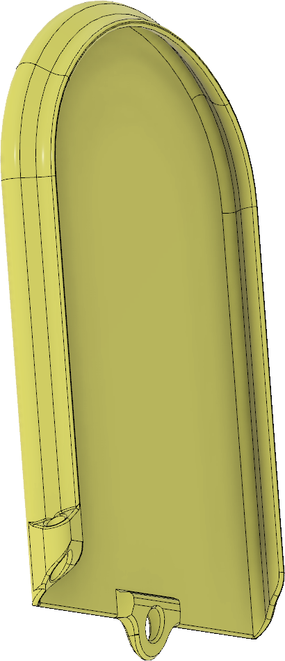
Locket som visas i Figur 22 skjuts som sagt på ovanifrån och omsluter de utstickande kanterna runt öppningen. Det blir inte vattentätt, men åtminstone rimliga mängder regn som kommer uppifrån bör hållas ute. Nedtill finns en klack som gör att locket snäpper fast, samt ett hål där man kan knyta ett snöre mellan locket och lådan så att de inte kommer bort från varandra.
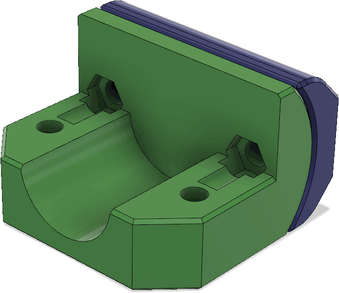
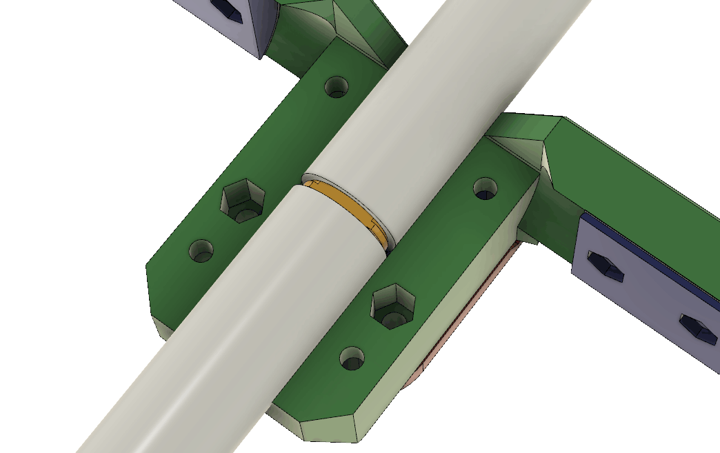
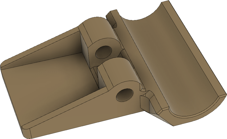
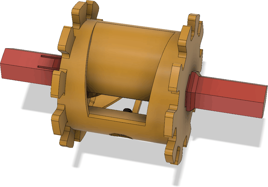
Mekanismen för att hålla fast lådan vid spjutet visas i Figur 23. Förutom delen som ingår i själva lådan finns en ledad klämma (orange) vars gångjärnspinne utgörs av en M4-skruv (syns inte i bilden), en M5-skruv med vingar (blå) och en rund, vridbar del med mutter (grön).
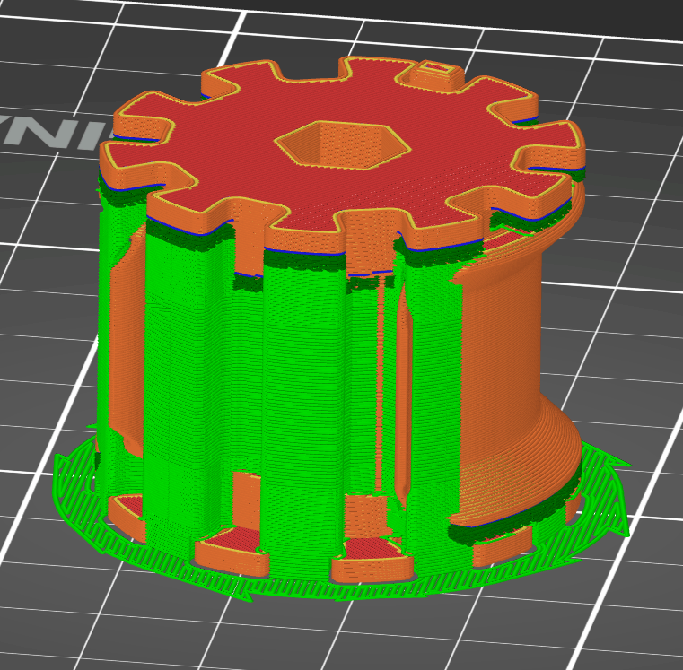
Lådorna jag skrivit ut hittills har blivit lite olika eftersom jag efter varje nytt exemplar kommit på någon förbättring att införa. Plasten jag använder är PETG som är seg, tål att vara utomhus, relativt billig och rätt lätt att skriva ut på de flesta 3D-skrivare. PLA som annars är vanlig i 3D-sammanhang kan nog inte rekommenderas eftersom den är ganska skör.
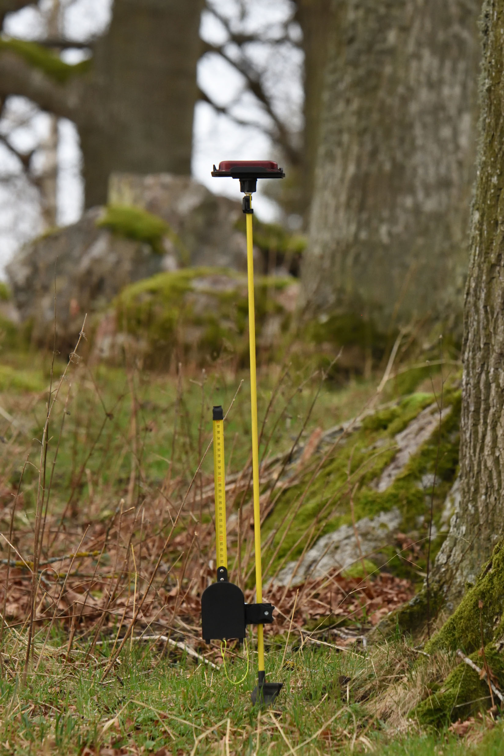
Hur det hela kan se ut när det är monterat på ett spjut framgår av Figur 24. För att det ska bli som på EM/VM ska antennen och spjutet målas svarta för att göra dem så svåra som möjligt att upptäcka för den som inte har full koll på pejlingen.
Bygg själv!
Om du vill bygga egna sändare av den här typen så finns programkod, underlag för mönsterkortet och 3D-modeller för lådan att ladda ned från [4]. Mönsterkorten går att beställa t.ex. från JLCPCB eller PCBWay. Om man vill ha en europeisk leverantör snarare än en kinesisk kan det vara värt att prova Aisler.
Möjliga förbättringar
Även om en del förbättringar redan är införda efter att jag tillverkade mina egna kort så finns det lite mer att göra om man vill. Här är några tankar:
- Byt till ett Chebyshev-filter som börjar och slutar med en spole i serie istället för en kondensator till jord. L4 lades in i ett sent skede och man skulle få bättre nytta av den om den ingick i Chebyshevfiltret. Utgångsspolen kan då eventuellt också kombineras med antennanpassningsspolen, vilket sparar in en spole.
- Det borde kunna bli tillräckligt bra (tillräcklig undertryckning av övertoner och tillräcklig effekt) utan att använda differentiell utgång (se del 1). Då slipper man den halvdyra balunen/transformatorn.
- Möjlighet att slå av matningen till LCD:n via mjukvara för att spara ström i ett eventuellt sovläge.
- Möjlighet att tända bakgrundsbelysningen till LCD:n vid väl valda tillfällen.
Programvara kan man alltid putsa på och det kräver inte nödvändigtvis några ändringar i hårdvaran. Tänkbara förbättringar är bland annat:
- Förbättringar i sigma-delta-moduleringen med högre ordnings modulator och optimerade egenskaper hos dithering-bruset.
- Optimering av strömförbrukningen. Kanske kan processorn sova mellan morsepipen?
- Stöd för sovläge och realtisklocka så att man kan programmera den att börja och sluta sända vid givna tillfällen utan att den drar mycket ström när den inte sänder.
Bruksanvisning
Jag har skrivit en kort bruksanvisning för satsen med 12 sändare jag byggt:
Referenser
[1] ”Foxoringsändare med Raspberry Pi Pico – del 1”, QTC nr 1, 2025
[2] ”RF Impedance Matching Calculator”, https://www.analog.com/en/resources/interactive-design-tools/rf-impedance-matching-calculator.html
[3] ”FoxScope – rävsax för 80 m med dubbla mottagarkedjor”, QTC nr 10 och 11, 2022
[4] Programkod och tillverkningsunderlag på Github: https://github.com/per-magnusson/RP2350-Foxoring-Transmitter/tree/main