|
|

|
This article is based on a presentation I held at a seminar organized by Würth and BK Services in Linköping 2012-10-01. The presentation described some findings from research I did at SP Devices. The presentation slides (in Swedish) are available here. Filtering of Power Supplies for Sensitive Analog ApplicationsPrefaceWhile this article describes a circuit solution to a power supply filtering problem, I think the main value of it is not the specific solution arrived at, but rather the methods used to get there as well as some general insights about how some components and circuits behave and how to utilize or mitigate that behavior. The method I use consists of both simulations (in LTspice) and measurements using a network analyzer. The solution is far from universally applicable since different applications have vastly different requirements in terms of current capability, maximum voltage drop allowed, amount of filtering required, cost, size etc. The methodology and general observations here are however hopefully more or less universally applicable to this kind of problem. The ProblemSometimes a power supply rail is needed that has very little noise *) on it. Such a supply rail may be required to improve the performance of e.g.:
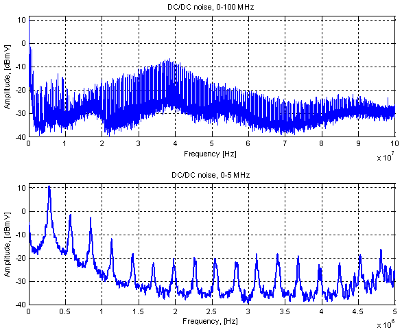
Switching AC/DC and DC/DC converters are often used to generate supply voltages in today's electronics, largely because they provide good efficiency even when the difference in input voltage to output voltage is big. These switchers are however notorious generators of noise, typically in the frequency range from a few hundred kHz up to at least several tens of MHz. Figure 1 below shows the spectrum of noise present on a supply generated by a DC/DC-converter switching at 280 kHz. As can be seen, the noise extends out to at least 100 MHz and it is composed mainly of harmonics of the 280 kHz switching frequency. Figure 1. Noise spectrum from a 280 kHz DC/DC
converter. (Click to enlarge.)
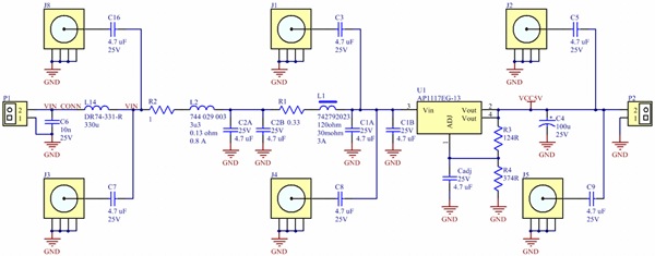
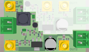
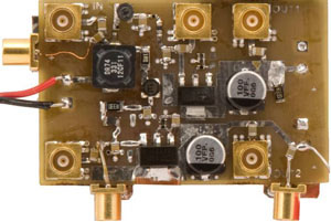
Other noise sources such as the mains AC frequency, variations in the mains voltage, I*R or L*di/dt drop modulated by fluctuating current consumption in the system can contribute disturbances with frequency components from less than a Hz and up to very high frequencies. Linear regulators provide cleaner outputs than switching regulators, but typically requirements on size, cost and power consumption often mandate the use of switching regulators in the system. So in order to provide a sub-circuit with a clean supply voltage, one is often faced with the problem of cleaning up the output of a swicthing converter. How can this be done? *) By noise I here mean both random noise as well as deterministic noise from e.g. DC/DC-converters, fluctuating mains voltages, perturbations generated by varying current consumption etc. Test BoardThere are a number of different strategies that one could follow to try to filter out the noise while maintaining a nice low-impedance supply rail. The two most obvious methods are perhaps LC-filters and linear regulators. LC-links can be configured as low-pass filters and attenuate higher frequencies while letting lower frequencies through. Linear regulators on the other hand generally have good supply rejection at low frequencies, while the rejection deteriorates as the frequency increases. A combination of an LC-filter and a linear regulator therefore seems like a good candidate solution to the problem. In order to test how well different configurations perform, I designed and built a test board that would allow me to use a (vector) network analyzer (VNA) to measure the filtering performance of a circuit aimed to deliver a low-noise 400 mA, 5 V supply. (A spectrum analyzer with a tracking generator would have worked as well as a VNA in this case as we are not interested in the phase of the transfer function.) Other requirements in this case was low cost and small size while high efficiency was not a major concern, so I could allow a few volts of drop over the filtering circuitry. The schematic and layout of the test board are shown in figures 2-4 below. Figure 2. Schematic of test board (click to enlarge).
Figures 3 and 4. 3D rendering and photo of test
board. The grayed-out parts of the board are not treated in this
article. (Click to enlarge.)
The board consists of:
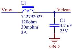
The board is 1.6 mm thick and made of standard FR4. It has two copper layers of which the bottom one is a solid ground plane. Most boards I do for real products have many more layers (at least 8) and this makes a bit of a difference in this application, at least at higher frequencies as the inductance of the vias from the top side down to the ground plane is increased due to the longer distance. Also, some undesired coupling paths may be stronger since the components and conductors are further away from the shielding ground plane. In general, the filtering is likely to be at least as effective on a multi-layer board as on this test board. A bit of a confession: The layout was done before I realized the utility of having dual coaxial connectors at each test point, so I had to patch in the extra connectors after the board was manufactured. This was made easier by the fact that the board has no solder mask and that the bottom side is a solid ground plane. Filtering Strategy 1 - FerriteFerrite beads are often used in various signal and power filtering applications. Sometimes the designer might have an overly strong confidence in the abilities of a ferrite, namely that it lets everything desired through and blocks everything that is undesired. Maybe there also exists a belief that circuits with ferrites never have resonances since one of their virtues is their loss (at high frequencies). The first filter we will examine is shown in figure 5 below and consists of a ceramic capacitor and a ferrite bead. The ferrite is part number 742792023 from Würth which is rated for 3 A and has an equivalent series resistance (ESR) of 30 mΩ. Figure 5. Schematic of ferrite filter. (Click to
enlarge.)
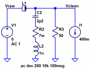
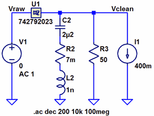
The filter is measured on the test board and also simulated in LTspice using the circuit shown in figure 6. Here I use the model for this particular ferrite that happens to be supplied with LTspice. I have also modeled the capacitor as a series LCR circuit. The reason the capacitance is 2.2 µF and not 4.7 µF is that the capacitance is voltage dependent and is reduced when the voltage increases. The resistance can be found in the datasheet for the capacitor while the inductance is a combination of the inductance of the capacitor and the layout (mainly the ground via). This value can be estimated through experience (see e.g. this article (in Swedish)) and if necessary tweaked so that the simulated response matches the measured response. The 50 Ω resistor is the impedance of the input port of the VNA and the current source is a crude model of the load (linear regulator). Figure 6. LTspice schematic of ferrite filter. (Click to enlarge.)
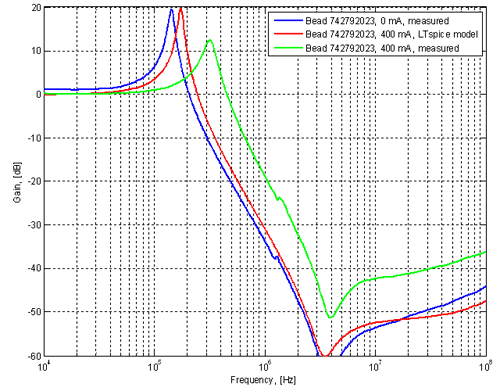
The results from simulation and measurements are shown in figure 7 below. Figure 7. Measured and simulated response of initial
ferrite filter. (Click to enlarge.)
A number of interesting things can be concluded from this experiment.
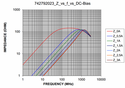
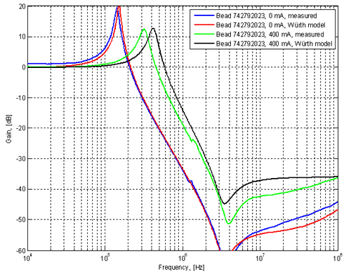
It turns out that Würth has published better LTspice models for some of their ferrites on their web site: http://www.we-online.de/web/en/passive_bauelemente_standard/toolbox_pbs/LTspice_III_IV.php. The behavior of this particular ferrite (742 792 023) is shown in the plot in figure 8. Figure 8. Impedance as a function of frequency and
bias current for ferrite 742792023 according to Würth. (Click to
enlarge.)
Replacing the ferrite model that came with LTspice with the one from Würth's web site, we get the circuit in figure 9 and the simulation results in figure 10. Figure 9. LTspice schematic with better ferrite model.
(Click to enlarge.)
Figure 10. Measured and simulated response of
ferrite filter using better model. (Click to enlarge.)
In figure 10 we can see a much better agreement between measured and simulated data. The plots for 0 mA are almost perfectly on top of each other. For 400 mA we see a little more inductance in reality than what the model indicates, but the general behavior of the curves are very similar. Apparently it is important to use the model downloaded from the manufacturer web site instead of the model shipped with LTspice if one is to get dependable simulation results for this component. Despite this extra hassle, it is nice to be able to with good accuracy simulate a component that behaves in such a relatively complex manner as a ferrite, since it allows us to make good predictions of the efficacy of various power filters without building and testing them. This can save both time and money. So, here are some conclusions about this particular ferrite filter.
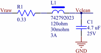
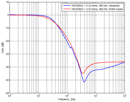
So, can we improve this filter to get rid of the peak? Filtering Strategy 2 - Dampened FerriteThe main problem with the ferrite filter above is that the losses are too small (the Q value is too high), so a resonance peak occurs. This increases the amplitude of the noise for a range of frequencies and we need to introduce loss to improve the situation. Loss means increased resistance and a resistor can be added either in series with the ferrite or in series with the capacitor. Adding it in series with the capacitor has the advantage that the DC drop over the filter does not increase, but the disadvantage that the maximum attenuation is much reduced as the capacitor-resistor combination can never have an impedance below the value of the resistor and so cannot short the signal arbitrarily well for any frequency. Another disadvantage is that the inductance to ground is increased, which also worsens the high frequency properties of the filter. An alternative to add a discrete resistor is to use a more lossy capacitor, like an electrolytic capacitor. This has the drawbacks of increased size and worse high-frequency performance as the inductance is typically much larger for an electrolytic than for a ceramic capacitor. Adding a resistor in series with the ferrite gets around these problems, but increases the DC drop. In the application at hand, a larger DC drop was permissible and therefore I went forward with that solution. Figure 11 below shows the modified filter and figure 12 shows the resulting simulated and measured response. The resistor value was chosen based on trial and error in the simulation as a tradeoff between getting rid of the peak while introducing as little resistance (and therefore DC drop) as possible. Figure 11. Dampened ferrite filter. (Click to enlarge.)
Figure 12. Simulated and measured response of
a dampened ferrite filter. (Click to enlarge.)
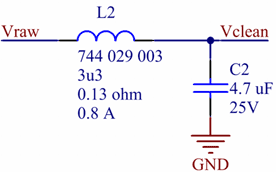
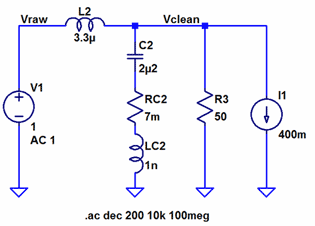
With the addition of the 0.33 Ω resistor, the peak is gone at the cost of increased DC drop. The agreement between simulation and measurement is decent. This resistor/ferrite/capacitor combination is not harmful at any frequency and is quite effective above 1 MHz. It is however insufficient for filtering a DC/DC-converter that switches at a few hundred kHz. In order to address noise at lower frequencies we need additional filtering and that can be addressed with a filter based on an inductor that has larger inductance than the ferrite. Filtering Strategy 3 - LC-filterThe LC filter schematic is shown in figure 13 and an LTspice version of it in figure 14. LTspice ships with a model for the inductor that was chosen here (Würth 744 029 003) and that model was used in the simulation. Figure 13. LC filter (Click to enlarge.)
Figure 14. LTspice model of LC filter. (Click to
enlarge.)
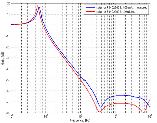
The filter was simulated and measured and the results are shown in the graphs of figure 15. Figure 15. Measured and simulated frequency response
of LC filter. (Click to enlarge.)
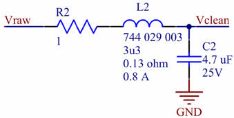
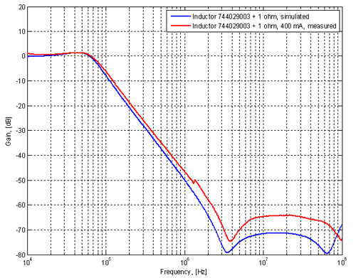
As one could guess from the results of the initial ferrite filter, there is an undesired peak in this filter as well. Other than that one can notice a good agreement between simulation and measurement. The filter starts to attenuate signals above around 100 kHz. If this had not been low enough, a larger inductor or capacitor could have been used. Apparently, the inductance of this inductor is not very dependent upon the DC bias current and the LTspice model works fine. There is also no better model of the inductor to be downloaded from the manufacturer. Filtering Strategy 3 - Dampened LC filterLike with the ferrite filter, we need to get rid of the peak and we try the same solution as previously, namely a series resistor. After a little bit of experimentation I opted for the value of 1 Ω. Schematic and test results are shown in figures 16 and 17 below. Figure 16. Dampened LC filter. (Click to enlarge.)
Figure 17. Measured and simulated frequency response
of dampened LC filter. (Click to enlarge.)
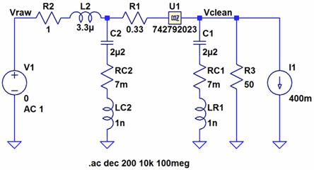
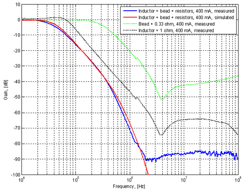
As previously, there is a tradeoff between dampening the peak and getting a larger DC drop. The next step is to combine the dampened ferrite and LC filters to one filter with better attenuation. Filtering Strategy 4 - Combined ferrite and LC filterFigures 18 and 19 show the combined filter schematics. The resulting frequency response, both simulated and measured is shown in figure 20 together with the responses of the individual filters for comparison. Simulation and measurement agree very well up to about 2 MHz. Above that the measurements indicate between 85 and 90 dB of attenuation whereas the simulation say that we should get even more attenuation. This discrepancy could in part be due to the measurement setup as well as coupling via paths that are not modeled. Anyway, 85 dB of attenuation is remarkably good, so we should not have much trouble with noise in the 2-100 MHz range getting through this filter. Figure 18. Dual link LC filter. (Click to enlarge.)
Figure 19. LTspice model of dual link LC filter.
(Click to enlarge.)
Figure 20. Measured and simulated frequency response
of combined filter and the two individual filter links for reference.
(Click to enlarge.)
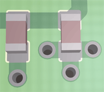
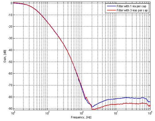
At 280 kHz (the DC/DC converter frequency in this case) we have about 35 dB of attenuation, which might not be good enough. Increaseing the capacitance or inductance in the LC-filter could help with this, but we will look at other solutions below, after first taking a little detour to look at layout effects. Layout EffectsAs mentioned above, the test board had two alternative layouts for the shunting capacitors. The two variants are shown in figure 21. Figure 21. Two layout variants for the shunting
capacitors. One GND via and three GND vias. (Click to enlarge.)
The two layouts were tested in the combined filter. First the two capacitors (one in each LC link) were placed on the footprints with one via and the response was measured (blue curve in figure 22) and then the two capacitors were moved to the footprints with three vias (red curve in figure 22). Figure 22. Plot showing the difference in attenuation
of dual-link LC filter when each capacitor has one GND via and when
they have three GND vias. (Click to enlarge.)
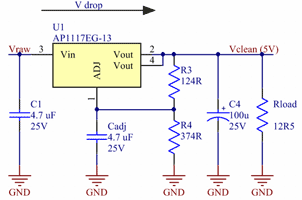
As can be seen, there is a noticeable effect of ~5 dB extra attenuation above the resonance frequency of the capacitors (~2 MHz). In the region below the capacitor resonance frequency, the capacitive reactance of the capacitors dominates the shunting sections and the reduced inductance makes no discernible difference. In this test board, the distance to the ground plane was the full board thickness of 1.6 mm, which makes the via inductance larger than on a typical multi-layer board, so the effect of adding more vias is more pronounced here than what one might encounter in a real application using a multi-layer PCB. One should also note that we probably have a significant measurement uncertainty at these high attenuations (80-90 dB), so the size of the magnitude of the difference in attenuation might be unreliable, although the fact that there is indeed an improvement above 2 MHz can be reliably concluded. Filtering Strategy 5 - Linear RegulatorSo far we have only looked at filtering techniques that reject high frequencies, but pass low frequencies. To clean up the lower part of the spectrum from DC and upwards we can use a linear regulator of some sort. In this particular application, it was important to keep the cost down, so a regulator called AP1117 from Diodes Inc was selected. The data sheet is quite sketchy and does not contain any ripple rejection plot. I have also been unable to find a Spice model for the regulator, so we have to do our own measurements in order to figure out the filtering performance. Looking at the data sheet for a similar regulator, LM1117 from Texas Instruments, I found a recommendation to bypass the lower resistor of the voltage setting resistive divider with a capacitor to improve ripple rejection. I therefore included this option in the design, despite the fact that the data sheet from Diodes Inc. did not mention it. The schematic is shown in figure 23. Figure 23. Schematic of linear regulator circuit.
(Click to enlarge.)
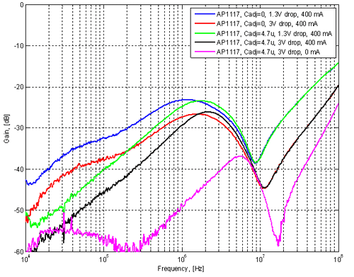
The measured frequency responses of the regulator for a number of different cases are shown in figure 24. Figure 24. Frequency response of AP1117 for a few
different cases. (Click to enlarge.)
A few parameters were varied to see how they affect the frequency response. The curves in figure 24 show the following cases:
Filtering Strategy 6 - LC-filters and Linear RegulatorWe have finally come to the point where it is time to combine the passive filters with the linear regulator. The full schematic is shown in figure 25. Figure 25. LC filter and linear regulator combined.
(Click to enlarge.)
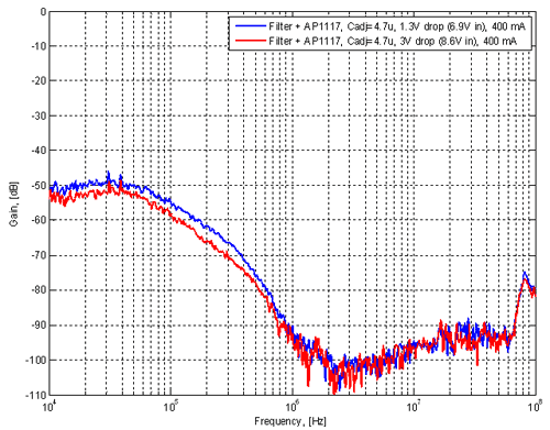
Measurement results are shown in figure 26 for both 3V drop and 1.3V drop over the regulator. Cadj was of course used and the load current was 400 mA as required by the application. Figure 26. Frequency response of combined LC filter
and regulator. (Click to enlarge.)
The main conclusions are:
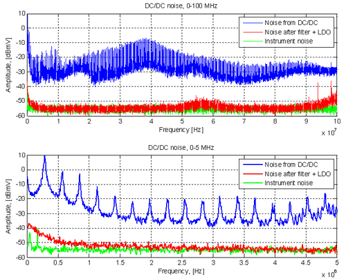
A test was done where the noise spectra from a 280 kHz DC/DC converter were measured before and after the filter. The results are shown in figure 27. Figure 27. Noise spectra from DC/DC converter before
and after filter. Upper plot shows 0 Hz to 100 MHz and lower plot
shows a zoom-in of 0 Hz to 5 MHz. (Click to enlarge.)
For comparison, the idle channel noise of the instrument is also plotted (green curve) and it shows that it is mostly the instrument noise floor that shows up in the curve after the filtering. In the zoomed-in view, one can however notice an interesting phenomenon. The red curve points up above the noise floor at low frequencies, but not following the shape of the blue noise spectrum. This noise is probably flicker noise generated by the regulator itself and might be something to watch out for if a very low noise supply is required. Better (and more expensive) regulators than AP1117 might have specifications for the output noise as well as a lower noise level. ConclusionsSo to summarize the findings in this article:
As mentioned at the beginning of this article, it is not the particular circuit that was developed here that is the main point of this article. For many applications it is certainly not particularly suitable and other requirements mandate other solutions using other components. Rather, the takeaway it to use simulation and (if possible) measurements to analyze the circuits instead of just throwing some components together and assuming they will work well. Some of the pitfalls to look out for are filter peaking, DC voltage drop, regulator characteristics and layout details. My hope is that the reader will be able to design better DC power filters after reading this text. |
| Updated: 2016-12-11, 14:28:23 |
|
![[SW flag]](pic/Sw_flag_40.png)

![[UK/US flag]](pic/UK-US_flag_40.png)

