![[SW flag]](pic/Sw_flag_40.png)

![[UK/US flag]](pic/UK-US_flag_40.png)

|
|

Design of an H BridgeOscilloscope plotsTo verify the operation of the H bridge (not the least to see that there is indeed no shoot-through), I looked at the gate voltages and the voltage drop over the current sense resistor using an oscilloscope. The resulting plots can be seen below. Unless something else is stated in the text the traces show the following signals:
The blue and yellow curves both have their offsets set to one division above the bottom of the plots whereas the green trace has its zero level two divisions below the top. It can be helpful to refer to the schematic PDF to more easily follow the descriptions of the phenomena that are observed in the plots. NMOS turning on while PMOS is off
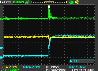
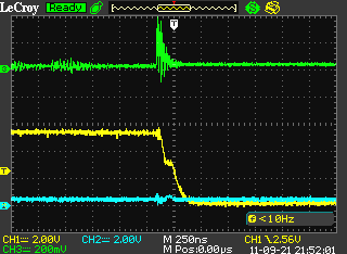
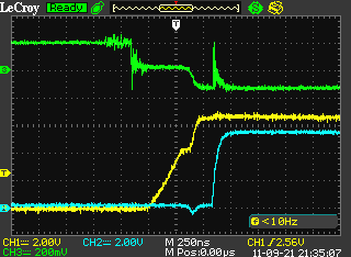
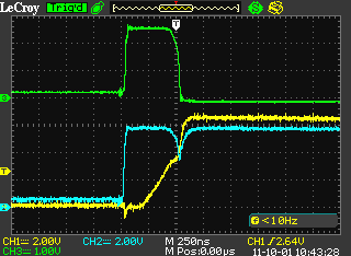
The NMOS transistor Q1A turns on while the PMOS Q1B
is off all the time, 250 ns/div and 1 ms/div.
There is no sudden step in the current when the transistor turns on since the inductance of the motor winding prevents sudden changes in current. It takes ~400 µs for the current to rise to close to its final value. NMOS turning off while PMOS is off
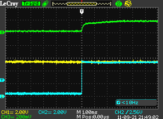
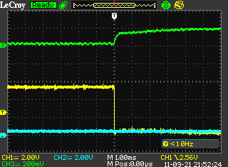
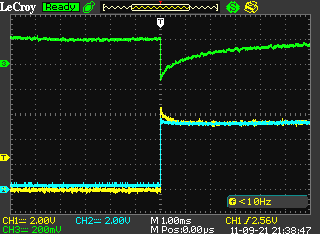
The NMOS transistor Q1A turns off while the PMOS Q1B
is off all the time, 250 ns/div and 1 ms/div.
Notice the ~400 µs long peak in the PMOS gate voltage after the NMOS turns off. What happens is that the NMOS stops conducting current, but the current in the large inductance of the motor continues to flow which very quickly raises the voltage at the drain of the PMOS until its body diode turns on. This sudden rise of the PMOS drain voltage couples into the gate of the PMOS through the gate-drain capacitance and raises the gate voltage. The emitter diode of Q5 is then back-biased and prevents the gate from being brought back to its original voltage. When the current in the winding has decayed to zero, the current also stops flowing in the body diode and the drain voltage suddenly goes down. This again couples to the gate which now returns to approximately its original voltage. Another phenomenon that can be observed is that the current through the sense resistor (green trace) first goes from 200 mA to 0 mA when the NMOS turns off and a little while later it goes to -200 mA and then decays slowly to 0. What happens here is that when the NMOS Q1A at the lower left turns off, the PMOS Q2B on the top right is still conducting since the PMOS drivers are slower than the NMOS drivers. As described above, the motor current starts flowing through the body diode of Q1B while it continues to flow through Q2B. During this period the current through the sense resistor is zero. 0.5 µs later the PMOS Q2B also turns off and the motor current needs to find another path. By sucking current from the drain node of the transistors to the right, the voltage at that node goes negative and current starts flowing through the body diode of Q2B until the current has decayed to zero, 400 µs later. PMOS turning on while NMOS is off
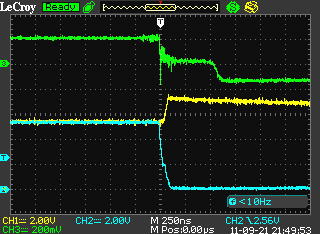
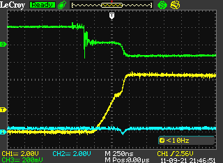
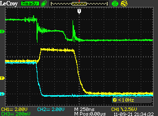
The PMOS transistor Q1B turns on while the NMOS Q1A is off
all the time, 250 ns/div and 1 ms/div
Notice the ~100 ns long plateau in the middle of the falling PMOS gate voltage. When the gate voltage of the PMOS falls, it quickly reaches the threshold voltage of the transistor and when that happens, the transistor starts conducting and quickly pulls the drain high. This rising drain voltage couples into the gate via the gate-drain capacitance and for a short while manages to counteract the current being pulled out of the gate capacitance via D5 and Q9. PMOS turning off while NMOS is off
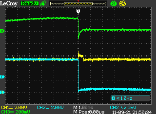
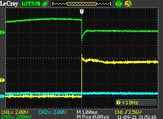
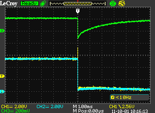
The PMOS transistor Q1B turns off while the NMOS Q1A is off
all the time, 250 ns/div and 1 ms/div
Here we see the same double-step behavior in the current through the sense resistor as we observed previously. The double step is again caused by the PMOS drivers being a little slower than the NMOS drivers. Here the NMOS transistor Q2A (whose gate voltage is not shown) turns off before the PMOS transistor turns off. That is the reason the current goes down to zero even before the PMOS gate voltage has changed at all. During this period when the sense voltage is zero, the current from the motor winding goes through the body diode of Q2B and the PMOS transistor Q1B which is still on. When the gate voltage of Q1B is high enough to reach the threshold voltage and it stops conducting, the current from the motor winding can no longer flow through the PMOS transistor Q1B and instead forces its drain voltage low until it starts pulling current through the body diode of Q1A. This is where the green trace (current) goes negative. The sudden step in drain voltage also couples through the parasitic gate-drain capacitance into the gate of the PMOS transistor Q1B and that is the reason for the plateau in the rising edge of the PMOS gate voltage trace. Polarity change, PMOS turning off, NMOS turning on
The PMOS transistor turns off and the NMOS turns on
(delayed by the asymmetrical delay circuit), 250 ns/div and 1 ms/div
The same thing happens here, namely that the NMOS transistor Q2A (whose gate voltage is not shown), turns off even before the gate voltage of PMOS Q1B starts changing and this is the reason the first thing that happens is that the current through the sense resistor initially goes to zero. The new thing here is that after the PMOS Q1B has turned off, NMOS Q1A turns on. The motor winding current then does not settle at zero once it has decayed, but instead builds up in the other direction than what it was first flowing in. It is a bit mysterious why it takes so much time (~5 ms) for the current to build up in this case whereas it took only a tenth of that time in the case above when the NMOS was turning on from a state where both transistors were off. The reason for the difference is probably that the motor was in different states when the two plots were taken. The position and movement of the rotor probably has an effect on the inductance and resistance of the windings (a device transforming electrical energy into mechanical energy must look at least somewhat resistive). Also, how the other windings are connected (or not) to the supply should matter. In the polarity reversal tests, the motor was driven in a way that all windings were powered at all times (except during the very brief period of polarity reversal), whereas in the on/off plots four of the windings were on and one was idle. This means that one winding was powered up and one was simultaneously powered down in those tests. Polarity change, NMOS turning off, PMOS turning on
The NMOS transistor turns off and the PMOS turns on
(delayed by the asymmetrical delay circuit), 250 ns/div
Here we see a polarity reversal, but in the opposite direction. The phenomena that can be observed here have mostly been discussed above. One can note that since the PMOS driver is slower than the NMOS driver, there is a larger gap between the switching of the two transistors in this case. Shoot-through
By shorting D13, shoot-through can be observed when
the gate voltages of Q1A and Q1B are rising.
Avoiding shoot-through was one of the design goals and it can be seen from the plots above that no shoot-through occurs during switching. To illustrate what it would look like if there were shoot-through, I shorted D13 so that the asymmetrical timing circuits became symmetrical. The result can be seen in the plot above. Notice that I had to change the scale of the current sense waveform so that it is now 1 A/div. What happens when D13 is shorted is that the NMOS transistor Q1A (whose gate voltage is the blue curve) turns on before its companion PMOS Q1B (yellow) has turned off. This results in 2.5A of short circuit current during 0.5 µs. © Per Magnusson, Axotron |
| Updated: 2016-12-11, 14:28:19 |
|