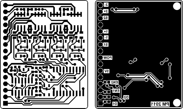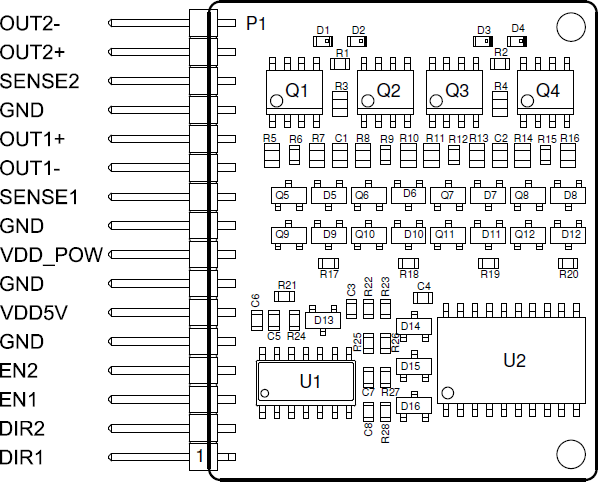
Figures 8 and 9 show the finished layout and figure 10 shows the assembly drawing. I like to work with surface mount components and all components except for the pin header are surface mount. The layout was done as a two layer board where most of the components are on the top layer and most of the bottom layer is a solid ground plane. Extensive gate and pin swapping was performed to simplify the layout and minimize the amount of tracks that would have to be placed on the bottom side and disrupt the ground plane. The pinout of the connector was also chosen to ease layout, but with signal and power integrity in mind.
![[PDF]](articles/H-Bridge/resources/pdf.png) The layout of the dual H bridge as a PDF.
The layout of the dual H bridge as a PDF.

![[PDF]](articles/H-Bridge/resources/pdf.png) The assembly drawing of the dual H bridge as a
PDF.
The assembly drawing of the dual H bridge as a
PDF.
I think the layout turned out all right as it is compact and pretty much limited by the size of the connector and the area of the components. It is good for EMC (electromagnetic compatibility, i.e. the ability to not disturb and not be disturbed through electromagnetic fields) that the ground plane is kept quite solid. The components that were chosen are all relatively thin (U2 is thickest at about 2.7 mm maximum) so several boards can be stacked tightly together.
The layout could however be made more compact if it were necessary. 0402 components could be chosen instead of 0603 and SC70/SOT323 packages might be available instead of the SOT23 packages that were used. U1 and U2 may also be available in smaller packages. I did however want to keep this design easy to assemble even without a microscope and that took priority over shrinking it further.
© Per Magnusson, Axotron