Igår fick jag för mig att jag skulle bygga en sittbänk att ha i trädgården, så jag köpte in lite virke, gjorde en ritning (i den ordningen) och satte igång att snickra. Det hela blev i stort sett klart under dagen. Bara någon mm trimning av ett ben för att den skulle stå helt plant och målning återstod till idag.
Så här blev resultatet:
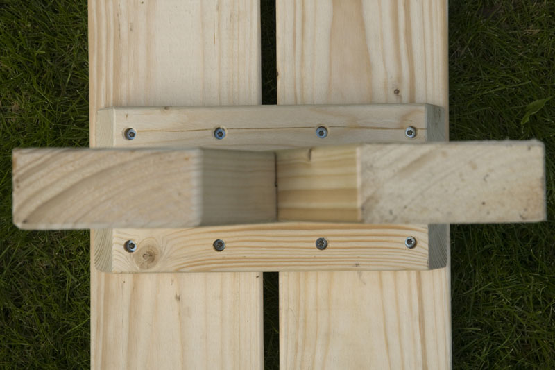
Den färdiga bänken innan målning.
Den som vill bygga något liknande kan kika på den här ritningen:
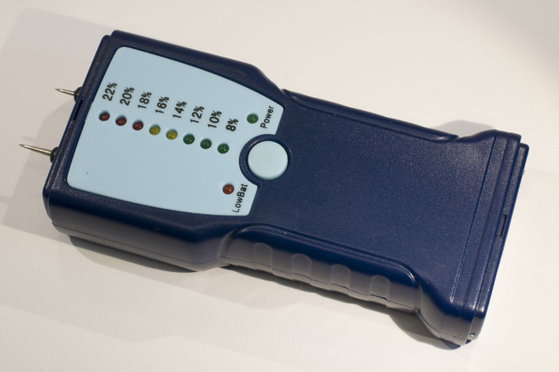
Yesterday, I bought a cheap moisture meter (“fuktmätare” in Swedish) called “Konkret MT210” (probably a rebranded name) in a local paint shop to measure the amount of moisture in wood to determine if it was dry enough to be painted.
Konkret MT210 moisture meter
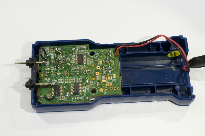
I started using it today, but after a few measurements, one of the two sharp pins that is used to probe the wood sunk into the meter and it became essentially useless. Not a good sign of quality.
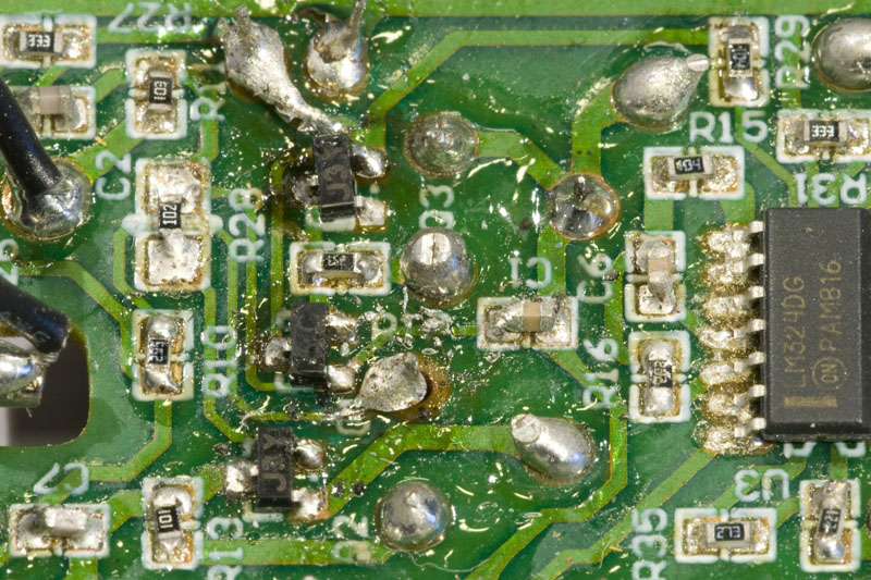
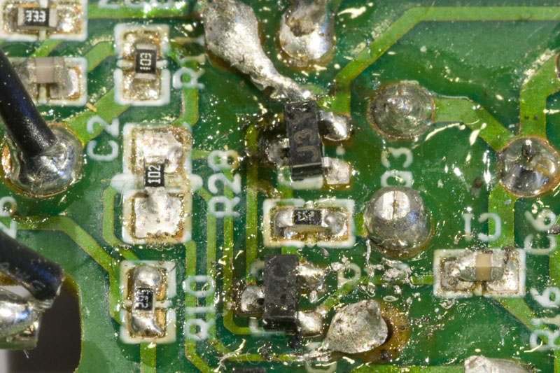
Before returning the faulty product to the shop, I decided to take it apart (it was kept together by four screws, so disassembly was straightforward) to see if it perhaps would be easy to fix it. The PCB inside it provided a surprise however. It was the most horrifically badly soldered circuit board I have ever seen. I do not even know how the manufacturer is able to produce such bad solder joints on an entire PCB. See below photos.
The innards of the moisture meter. Note how the lower probe has been pushed inwards.Close-up of badly soldered PCB.Even closer up of the ugly PCB.
Misaligned components, lots of solder residue, excess solder, many lose solder blobs and even missing copper pads. It is not a pretty sight.
So not only was this product mechanically deficient, the electronics was also built using some entirely inadequate process. I do not recommend anyone to buy this product.
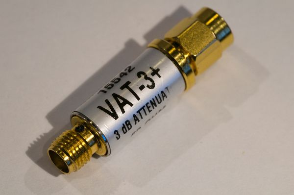
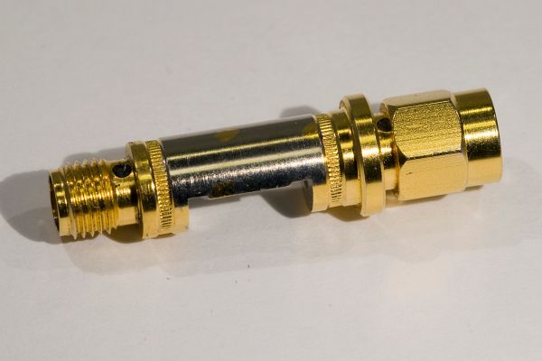
I came across a broken 3 dB attenuator and since I was curious of its internal design, I decided to do an autopsy, just like I did with the broken termination a few months ago. The attenuator is made by Mini-Circuits and it is a low-cost type useful up to 6 GHz. The manufacturer part number is VAT-3+. The data sheet says it costs $13.95.
VAT-3+ attenuator
The symptoms were that the female connector was an open circuit (bad) while the male connector had a resistance of 150 ohms to ground (which is what it should be for a 3 dB attenuator). This indicated an open circuit between the female connector and the internal resistive network.
It is perhaps not obvious how to take the attenuator apart, but I decided to start filing on the central tube (which seemed to be made out of brass) in the hope that I would then be able to pry it apart to reveal the interior.
An opening has been filed into the enclosure and the innards can be glimpsed.
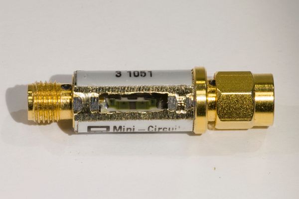
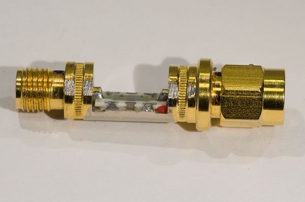
This turned out to be successful and I could soon remove the tube. An alternative (maybe easier?) method might have been to remove the label and then drill out the four punch marks around the rims of the tube.
The tube has been removed.
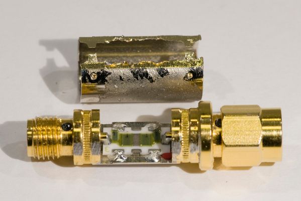
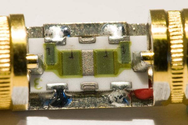
Inside the attenuator, there is a small substrate with four laser trimmed thick film resistors forming the pi-topology attenuator. See my article about pi and T attenuators for more information about attenuator design.
The attenuator contains a continuous brass structure making up both connectors as well as the base on which the substrate is mounted.The attenuator substrate viewed from the side.The substrate from the top. The dark L-shapes into the green thick film resistors are probably the marks left by laser trimming.
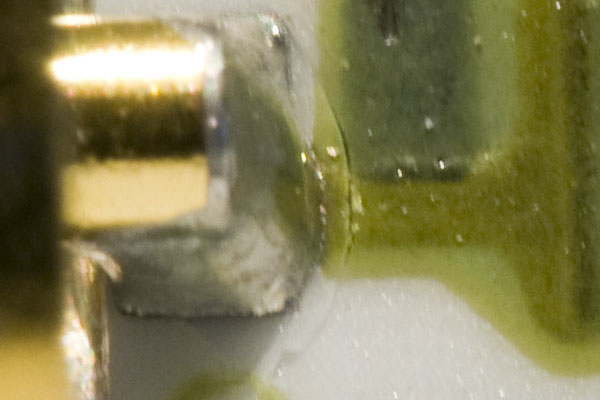
At first glance it was not obvious what was broken inside the device, but there had to be a crack or something between the left connector terminal and the substrate in the photo above. If one looks carefully, it is possible to see that there is indeed a crack around the solder joint. The photo below shows a zoomed in version where the microscopic crack is quite visible.
The crack that prevents the attenuator from working.
A possible cause for the crack is if an SMA connector with a misaligned center pin was forced into the connector of the attenuator, causing the terminal to be pushed harder towards the substrate than what it could handle.
So, this is what Mini-Circuits’ low-cost 1 W attenuators look like inside. A custom machined brass body onto which a substrate with laser trimmed resistors are mounted.


![[PDF]](http://axotron.se/blog/wp-content/uploads/2015/05/pdfbig.png) Ritningen som PDF
Ritningen som PDF